

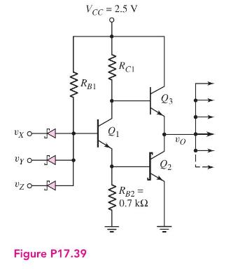
Consider the modified Schottky TTL NAND gate shown in Figure P17.39. The current gain of all transistors
Question:
Consider the modified Schottky TTL NAND gate shown in Figure P17.39. The current gain of all transistors is \(\beta=20\).
(a) Assume \(v_{X}=v_{Y}=v_{Z}=\) logic 1 and assume two similar type load circuits are connected to the output. The transistor \(Q_{2}\) is biased in saturation with \(i_{B 2}=0.1 \mathrm{~mA}\) and \(i_{C 2}=0.2 \mathrm{~mA}\). Determine the values of \(R_{B 1}\) and \(R_{C 1}\).
(b) Using the results of part (a), and assuming \(v_{X}=0.4 \mathrm{~V}\) and \(v_{Y}=v_{Z}=1.8 \mathrm{~V}\), determine \(v_{B 1}\), \(v_{B 2}, v_{O}\), and all base and collector currents. Assume two similar type load circuits are connected to the output.
(c) Assume \(v_{X}=v_{Y}=v_{Z}=\) logic 1 and assume four similar type load circuits are connected to the output. Using the results of part (a), determine \(v_{B 1}, v_{B 2}, v_{O}\), and all base and collector currents.
(d) Determine the maximum fanout for a low output state.
Step by Step Answer:


Microelectronics Circuit Analysis And Design
ISBN: 9780071289474
4th Edition
Authors: Donald A. Neamen
