

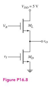
The enhancement-load transistor in the NMOS inverter in Figure P16.8 has a separate bias applied to the
Question:
The enhancement-load transistor in the NMOS inverter in Figure P16.8 has a separate bias applied to the gate. Assume transistor parameters of \(K_{n}=1 \mathrm{~mA} / \mathrm{V}^{2}\) for \(M_{D}, K_{n}=0.4 \mathrm{~mA} / \mathrm{V}^{2}\) for \(M_{L}\), and \(V_{T N}=1 \mathrm{~V}\) for both transistors. Using the appropriate logic 0 and logic 1 input voltages, determine \(V_{O H}\) and \(V_{O L}\) for:
(a) \(V_{B}=4 \mathrm{~V}\),
(b) \(V_{B}=5 \mathrm{~V}\),
(c) \(V_{B}=6 \mathrm{~V}\), and
(d) \(V_{B}=7 \mathrm{~V}\).
Fantastic news! We've Found the answer you've been seeking!
Step by Step Answer:

Answered By
ANDREW KIPRUTO
Academic Writing Expert
I have over 7 years of research and application experience. I am trained and licensed to provide expertise in IT information, computer sciences related topics and other units like chemistry, Business, law, biology, biochemistry, and genetics. I'm a network and IT admin with +8 years of experience in all kind of environments.
I can help you in the following areas:
Networking
- Ethernet, Wireless Airmax and 802.11, fiber networks on GPON/GEPON and WDM
- Protocols and IP Services: VLANs, LACP, ACLs, VPNs, OSPF, BGP, RADIUS, PPPoE, DNS, Proxies, SNMP
- Vendors: MikroTik, Ubiquiti, Cisco, Juniper, HP, Dell, DrayTek, SMC, Zyxel, Furukawa Electric, and many more
- Monitoring Systems: PRTG, Zabbix, Whatsup Gold, TheDude, RRDtoo
Always available for new projects! Contact me for any inquiries
1+ Reviews
10+ Question Solved
Related Book For 

Microelectronics Circuit Analysis And Design
ISBN: 9780071289474
4th Edition
Authors: Donald A. Neamen
Question Posted:
