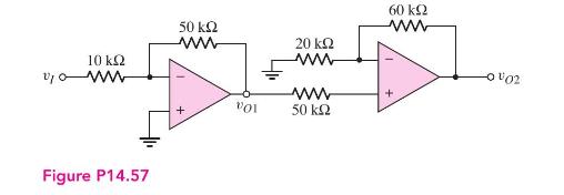
The input offset voltage in each op-amp in Figure P14.57 is (V_{O S}=1 mathrm{mV}) at (T=25^{circ} mathrm{C})
Question:
The input offset voltage in each op-amp in Figure P14.57 is \(V_{O S}=1 \mathrm{mV}\) at \(T=25^{\circ} \mathrm{C}\) and the input offset voltage coefficient is \(\mathrm{TC} v_{O S}=3.3 \mu \mathrm{V} /{ }^{\circ} \mathrm{C}\). Find the worst-case output voltages \(v_{O 1}\) and \(v_{O 2}\) at:
(a) \(T=25^{\circ} \mathrm{C}\) and
(b) \(T=50^{\circ} \mathrm{C}\).

Fantastic news! We've Found the answer you've been seeking!
Step by Step Answer:
Related Book For 

Microelectronics Circuit Analysis And Design
ISBN: 9780071289474
4th Edition
Authors: Donald A. Neamen
Question Posted:


