

Question: The transistor parameters for the common-source circuit in Figure P4.59 are (V_{T N D}=0.4 mathrm{~V}, quad V_{T P L}=-0.4 mathrm{~V}, quad(W / L)_{L}=50, quad lambda_{D}=0.02
The transistor parameters for the common-source circuit in Figure P4.59 are \(V_{T N D}=0.4 \mathrm{~V}, \quad V_{T P L}=-0.4 \mathrm{~V}, \quad(W / L)_{L}=50, \quad \lambda_{D}=0.02 \mathrm{~V}^{-1}\), \(\lambda_{L}=0.04 \mathrm{~V}^{-1}, k_{n}^{\prime}=100 \mu \mathrm{A} / \mathrm{V}^{2}\), and \(k_{p}^{\prime}=40 \mu \mathrm{A} / \mathrm{V}^{2}\). At the \(Q\)-point, \(I_{D Q}=0.5 \mathrm{~mA}\).
(a) Determine \((W / L)_{D}\) such that the small-signal voltage gain is \(A_{v}=V_{o} / V_{i}=-40\).
(b) What is the required value of \(V_{B}\) ?
(c) What is the value of \(V_{G S D Q}\) ?
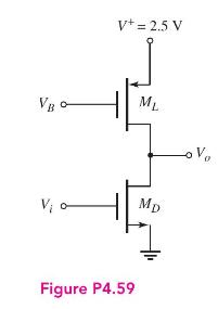
VB V+= 2.5 V T ML MD Vo Vo Figure P4.59
Step by Step Solution
There are 3 Steps involved in it

Get step-by-step solutions from verified subject matter experts