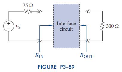
The circuit in Figure P389 has a source resistance of 75 V and a load resistance of
Question:
The circuit in Figure P3–89 has a source resistance of 75 V and a load resistance of 300 V. Design the interface circuit so that the input resistance is RIN ¼ 75 V 10% and the output resistance is ROUT ¼ 300 V 10%.
Fantastic news! We've Found the answer you've been seeking!
Step by Step Answer:
Related Book For 

The Analysis And Design Of Linear Circuits
ISBN: 9781118214299
7th Edition
Authors: Roland E Thomas, Albert J Rosa, Gregory J Toussaint
Question Posted:


