

Question: A MOS current source of the type shown in Fig. 4.4 is to be designed to achieve minimum output current noise. The two transistors must
A MOS current source of the type shown in Fig. 4.4 is to be designed to achieve minimum output current noise. The two transistors must be identical and the total gate area of the two transistors combined must not exceed 10 µm2. Choose the W and Lof the devices under two different assumptions:
(a) 1/f noise dominates.
(b) Thermal noise dominates.
Assume that Ld and Xd are zero. The minimum allowed transistor length or width is 0.6 µm. Verify your design using SPICE.
Fig. 4.4:
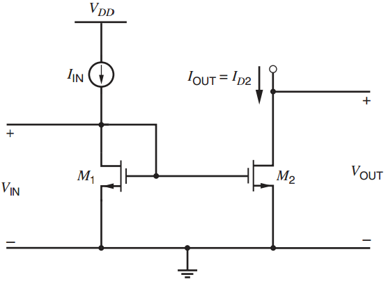
VDD IIN IOUT = ID2 VOUT M2 M1 VIN
Step by Step Solution
3.31 Rating (175 Votes )
There are 3 Steps involved in it
a Maximize L to minimize 1f noise W 1 06 m ... View full answer

Get step-by-step solutions from verified subject matter experts
Document Format (2 attachments)
1528_605d88e1c186a_687025.pdf
180 KBs PDF File
1528_605d88e1c186a_687025.docx
120 KBs Word File