

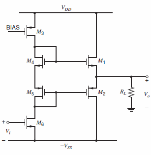
Question: Design a CMOS output stage based on the circuit of Fig. 5.31 to deliver ±1 V before clipping at V o with R L =
Design a CMOS output stage based on the circuit of Fig. 5.31 to deliver ±1 V before clipping at Vowith RL = 1 kΩ and VDD= VSS= 2.5 V. Use 10 µA bias current in M3and 100 µA idling current in M1and M2. Set (W/L)3= 50/1 and (W/L)6= 25/1. Specify the W/L for M1-M6that minimizes the total chip area. Use the transistor parameters in Table 2.3 except assume that Leff= Ldrwnfor simplicity. The minimum channel length is 1 µm. Assume the body of each n-channel transistor is connected to ˆ’VSS, and the body of each p-channel transistor is connected to VDD. Use SPICE to verify your design by plotting the Voversus Vicharacteristic.
Figure 5.31:
VDp BIAS M4 V. RL M2 M5. M6 V; -Vss
Step by Step Solution
3.47 Rating (176 Votes )
There are 3 Steps involved in it
008 2 fn 650 mV 2 fp 750 mV Table 23 K n 127 AV K P 58 AV V tn 07 V V ... View full answer

Get step-by-step solutions from verified subject matter experts
Document Format (2 attachments)
1528_605d88e1b2f5b_686874.pdf
180 KBs PDF File
1528_605d88e1b2f5b_686874.docx
120 KBs Word File