

Answered step by step
Verified Expert Solution
Question
1 Approved Answer
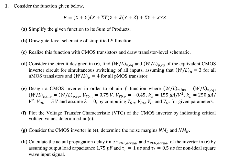
1. Consider the function given below, F = (X+Y)(X + XY)Z + X(Y + 7) + XY + XYZ (a) Simplify the given function to
Step by Step Solution
There are 3 Steps involved in it
Step: 1

Get Instant Access to Expert-Tailored Solutions
See step-by-step solutions with expert insights and AI powered tools for academic success
Step: 2

Step: 3
Ace Your Homework with AI
Get the answers you need in no time with our AI-driven, step-by-step assistance
Get Started
Preliminary Audit Results Montanas State Employee Compensation 1990
Authors: Waters Consulting Group, Montana. State Employee Compensation Committee
1st Edition
1378152700, 978-1378152706