

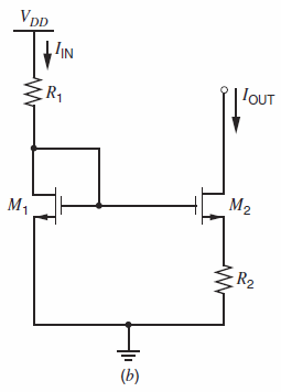
Question: Design a MOS Widlar current source using the circuit shown in Fig. 4.31b to meet the following constraints with V DD = 3 V: (a)
Design a MOS Widlar current source using the circuit shown in Fig. 4.31b to meet the following constraints with VDD= 3 V:
(a) The input current should be 100 µA, and the output current should be 10 µA.
(b) Vov1 = 0.2 V.
(c) Transistor M2 must operate in the active region if the voltage from the drain of M2 to ground is at least 0.2 V.
(d) The output resistance should be 50 MΩ.
Ignore the body effect. Assume Ldrwn = 1 µm and Xd = Ld = 0. Use Table 2.4 for other parameters.
Fig. 4.31 (b):
VDD IN IOUT ER, M2 M1 R2 (b)
Step by Step Solution
3.53 Rating (170 Votes )
There are 3 Steps involved in it
Ignore BEX d L d 0 R o r o2 1 g m2 R 2 R o 5... View full answer

Get step-by-step solutions from verified subject matter experts
Document Format (2 attachments)
1528_605d88e1af438_686835.pdf
180 KBs PDF File
1528_605d88e1af438_686835.docx
120 KBs Word File