

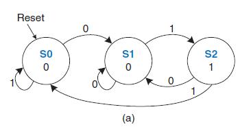
Question: Repeat Exercise 8.29 for the FSM in Figure 3.30(a). The input A and output Y are memory-mapped to bits 0 and 1, respectively, of address
Repeat Exercise 8.29 for the FSM in Figure 3.30(a). The input A and output Y are memory-mapped to bits 0 and 1, respectively, of address 0xFFFFF040.
Figure 3.30(a
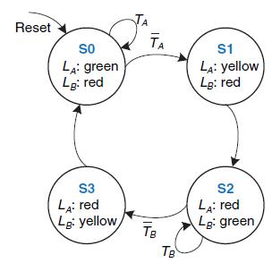
(a) Implement the traffic light FSM from Figure 3.25 using MIPS assembly code. The inputs (TA and TB) are memory-mapped to bit 1 and bit 0, respectively, of address 0xFFFFF000. The two 3-bit outputs (LA and LB) are mapped to bits 0–2 and bits 3–5, respectively, of address 0xFFFFF004. Assume one-hot output encodings for each light, LA and LB; red is 100, yellow is 010, and green is 001.
Figure 3.25
(b) Draw a schematic for this memory-mapped I/O system.
(c) Write HDL code to implement the address decoder for your memory-mapped I/O system.
Reset so S1 S2 (a)
Step by Step Solution
3.32 Rating (161 Votes )
There are 3 Steps involved in it
a b c Address Decoder SystemVerilog VHDL MIPS code for Snail FSM addi t1 0 1 addi 12 0 2 SW 0 ... View full answer

Get step-by-step solutions from verified subject matter experts