

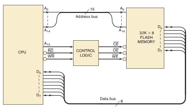
Question: Figure 12-42 shows a small flash memory chip connected to a CPU over a data bus and an address bus. The CPU can write to
Figure 12-42 shows a small flash memory chip connected to a CPU over a data bus and an address bus. The CPU can write to or read from the flash memory array by sending the desired memory address and generating the appropriate control signals to the chip. The CPU asserts the R̅D̅ line when it has finished outputting a stable address and wants to read data from the memory device. The CPU asserts the W̅R̅ line after it has finished outputting a stable address and has placed the data to be stored on the data bus.
(a) What control logic is needed to allow this flash memory array to occupy addresses between 800016 and FFFF16?
(b) Which bus will carry the command codes from the CPU to the flash memory chip?
(c) What type of bus cycle will be executed to send control codes to the flash memory chip?
Figure 12-42
CPU 8111115 Do Ao A14 A15 RD WR 15 Address bus CONTROL LOGIC A14 CE OE WE Data bus 8 32K X 8 FLASH MEMORY 1 1 1 1
Step by Step Solution
3.47 Rating (147 Votes )
There are 3 Steps involved in it
a To allow the flash memory array to occupy addresses between 800016 and FFFF16 the following contro... View full answer

Get step-by-step solutions from verified subject matter experts