

Question: THE REQUIREMENTS DOCUMENTS ARE AS FOLLOWS: PLEASE PROVIDE OP CODE TABLE & MACHINE CYCLE DIAGRAM IN EXCEL OR PDF Either Word, Visio, PDF, or any

THE REQUIREMENTS DOCUMENTS ARE AS FOLLOWS:
PLEASE PROVIDE OP CODE TABLE & MACHINE CYCLE DIAGRAM IN EXCEL OR PDF
Either Word, Visio, PDF, or any acceptable format that clearly shows a block diagram of the MICROarchitecture.
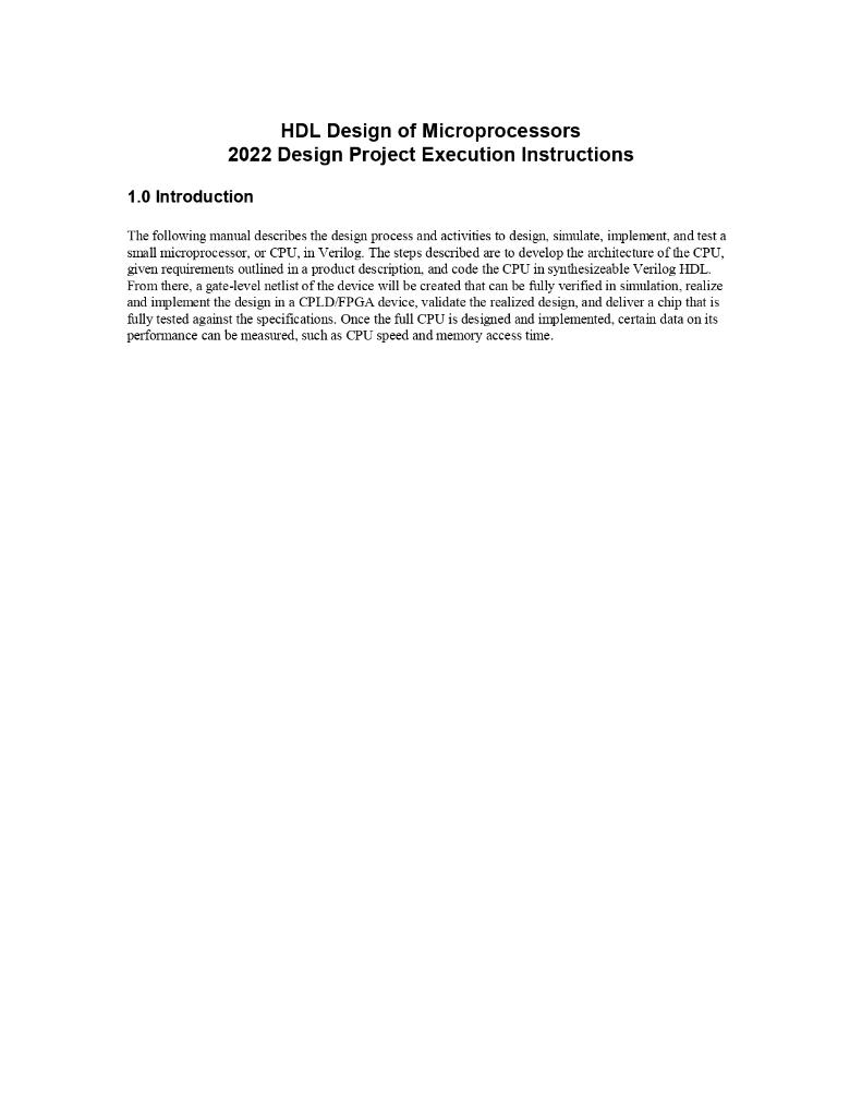
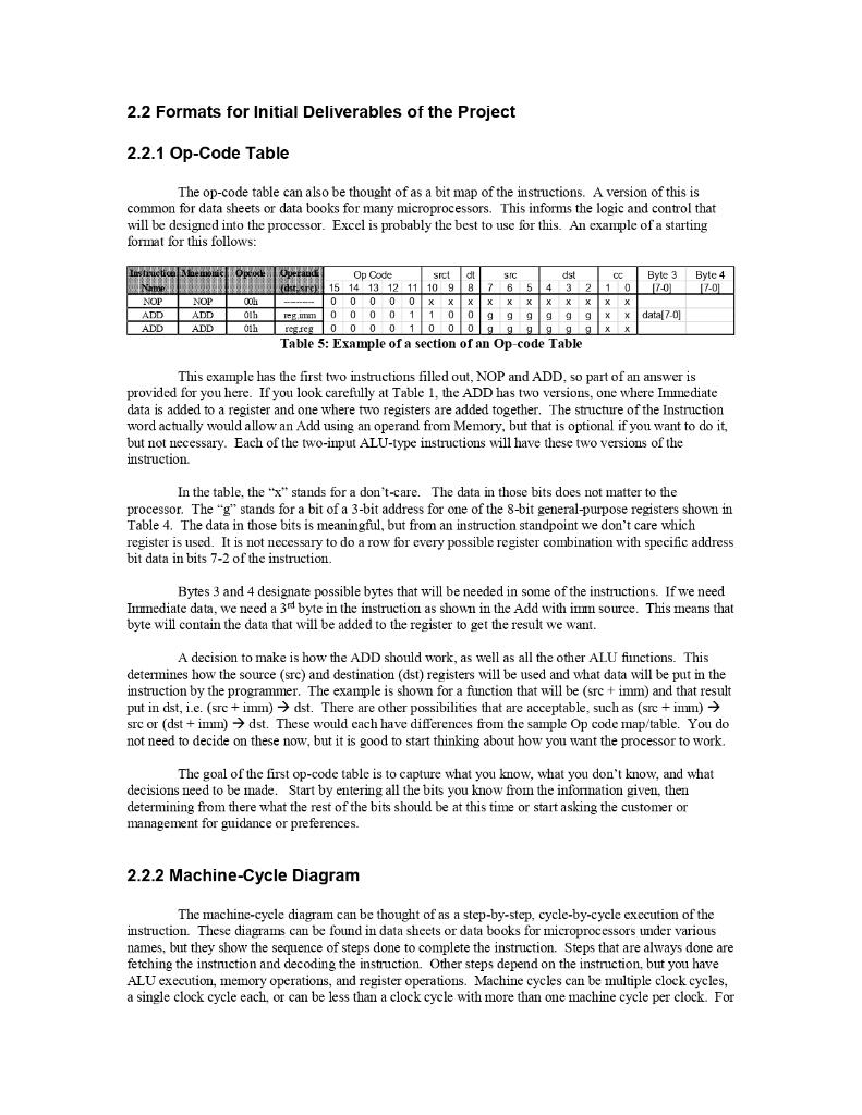
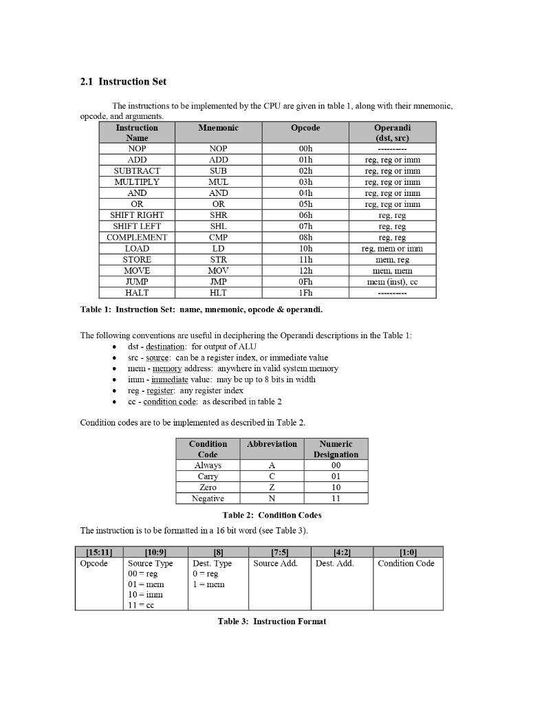
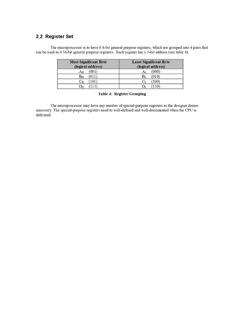
HDL Design of Microprocessors 2022 Design Project Execution Instructions 1.0 Introduction The following manual describes the design process and activities to design, similate, implement, and test a small microprocessor, or CPU, in Verilog. The steps described are to develop the architecture of the CPU, given requirements outlined in a product description, and code the CPU in synthesizeable Verilog HIDL. From there, a gate-level netlist of the device will be created that can be fully verified in simulation, realize and implement the design in a CPLD/FPGA device, validate the realized design, and deliver a chip that is fully tested against the specifications. Once the full CPU is designed and implemented, certain data on its performance can be measured, such as CPU speed and memory access time. 2.0 Initial Start-Up of the Project 2.1 Understanding and Expanding on the Requirements Your initial work on the project should be directed at first analyzing and understanding the requirements for the microprocessor. Review the requirements document and note any terins or concepts that you may not understand. Ask the customer or manager to explain them in this case, it would be the course instructor). Make sure you note what is required, what is optional, what design constraints you may have, and what design leeway you may have. The first tangible activity should be to review the instruction set and understand how it needs to work in detail when the design is completed. The best way is to analyze and depict the bit-by-bit coding of each instruction. A good way to do this is with an op-code table (or matrix). This shows each instruction with the value for each of the 16 bits in the instruction. A second item that you will need is outlining a machine-cycle definition of each instruction's execution - so you are clear on how each instruction is to be executed. The machine-cycle here denotes the complete cycle of executing the instruction, usually depicted in a clock-by-clock manner or edge-by-edge mamer (e.g. clock rise, then clock fall, next clock rise, etc.). The complete machine-cycle starts with retrieving the instruction from program memory (typically ROM) and ends with completion of the that retrieved instruction, and the processor is ready to start the next machine-cycle. Keep the following in mind as you do this for this project: Since each instruction is 16 bits in width, all instructions will need two fetch cycles. Instructions returning 16-bit results will need to be ended with two write cycles, to two different 8-bit registers (as discussed section 1.1.2). It is not necessary to pipeline instruction execution. . As you are defining the execution of each instruction, you will also architect the part. In VLSI design, this is typically called micro-architecture. Micro-architecture helps you to define all the blocks of your system, all the signals that connect them, the flow of data through your system, etc. It is very important that this task be done very carefully, as it will in large part determine the success or failure of the project. You should compare this architecture with the execution each instruction, as depicted in your machine-cycle diagram and verify that this architecture allows each instruction to execute as intended. Think through in your mind how data flows from block to block, how instructions are executed, etc., and verify that each instruction can be completed. One of the first things to do in defining the architecture is to define the inputs and outputs (I/O's); that is, the power and signal pins, but primarily the signal pins. After that, develop a diagram to depict the blocks, define the basic finctionality of each block, and interconnect these blocks After you have done the above and established a good design foundation, you will begin coding each of the blocks in Verilog HDL - and this begin the physical realization of your processor. The micro- architecture diagram will be your guide as you interconnect these blocks and define the functionality of each in Verilog. Focus the first week on getting these tasks done. Your deliverables are a Rev 0 or Version 1 ("first draft") op-code table, Rev O machine-cycle diagram, and Rev O micro-architecture diagram that allows each instruction in the machine-cycle diagram to be executed. We will use the nomenclature v.x.x to track our revisions, so this first one will be v.1.0. Major revisions will increment the first number and minor revisions will increinent the second number 2.2 Formats for Initial Deliverables of the Project 2.2.1 Op-Code Table The op-code table can also be thought of as a bit map of the instructions. A version of this is common for data sheets or data books for many microprocessors. This informs the logic and control that will be designed into the processor. Excel is probably the best to use for this. An exanple of a starting format for this follows: Instructice Meteo Operandi Op Code srct dt HAMA Kastre 15 14 13 12 11 10 9 8 7 6 5 SIC dst CC Byte 3 Byle 4 NADOR - 4 3 2 10 170 17-01 NOP NOP ook O011 0 0 0 0 0 0 x x x x Xxx x x X X X X X ADD ADD Olh Term 0 0 0 0 0 0 0 1 11 0 0 ggggg 99 g x x data[7-01 ADD ADD OLE reg.seg 0 0 0 0 1 0 0 0 0 0 9_9_legg X X gxX Table 5: Example of a section of an Op-code Table This example has the first two instructions filled out, NOP and ADD, so part of an answer is provided for you here. If you look carefully at Table 1, the ADD has two versions, one where Immediate data is added to a register and one where two registers are added together. The structure of the Instruction word actually would allow an Add using an operand from Memory, but that is optional if you want to do it, but not necessary. Each of the two-input ALU-type instructions will have these two versions of the instruction. In the table, the *x** stands for a don't care. The data in those bits does not matter to the processor. The "g" stands for a bit of a 3-bit address for one of the 8-bit general-purpose registers shown in Table 4. The data in those bits is meaningful, but from an instruction standpoint we don't care which register is used. It is not necessary to do a row for every possible register combination with specific address bit data in bits 7-2 of the instruction. Bytes 3 and 4 designate possible bytes that will be needed in some of the instructions. If we need Innediate data, we need a 3 byte in the instruction as shown in the Add with inm source. This means that byte will contain the data that will be added to the register to get the result we want. A decision to make is how the ADD should work, as well as all the other ALU functions. This determines how the source (sic) and destination (dst) registers will be used and what data will be put in the instruction by the programmer. The example is shown for a function that will be (src + imm) and that result put in dst, i.e. (src + imm) dst. There are other possibilities that are acceptable, such as (src + imm) src or (dst + imm) dst. These would each have differences from the sample Op code map/table. You do not need to decide on these now, but it is good to start thinking about how you want the processor to work. The goal of the first op-code table is to capture what you know, what you don't know, and what decisions need to be made. Start by entering all the bits you know from the information given, then determining from there what the rest of the bits should be at this time or start asking the customer or management for guidance or preferences. 2.2.2 Machine-Cycle Diagram The machine-cycle diagram can be thought of as a step-by-step, cycle-by-cycle execution of the instruction. These diagrams can be found in data sheets or data books for microprocessors under various names, but they show the sequence of steps done to complete the instruction. Steps that are always done are fetching the instruction and decoding the instruction. Other steps depend on the instruction, but you have ALU execution memory operations, and register operations. Machine cycles can be multiple clock cycles, a single clock cycle each, or can be less than a clock cycle with more than one machine cycle per clock. For this design, we will just go with a single clock per machine cycle or single machine cycle per clock, whichever way you like to think about it. Excel and Word are both tools that can be used for this, and the result is probably best shown in a table format or a sequence diagram. The following is a table format: Mie monk Instruction Name MG NOP NOP Quick Machine Cycles No M1 M2 M3 M4 M5 Instruction Instruction Execute Felch 1 Inext inst) Felch 2 NOP? Fetch SIC - Instruction Instruction Fetch 1 Fetch 2 Immediate Execute ADD Store Resut in Dest. Reg Data Table 6: Example of a section of a Machine-Cycle Diagram ADD ADD next inst) This shows the sample format and a NOP and one of the ADD instructions (ADD with immediate). All instructions will need two Instruction Fetches (16-bit instruction and 8-bit data bus), so you already have the answer for every instruction for the first two cycles (or first two clocks). The NOP can either just go to the next instruction or execute a "dead clock, i.e. nothing happens for a clock/cycle, then go to the next instruction. The ADD with src=imm needs to do the two Instruction Fetches, then go get the next byte, which has the Immediate data. Once it has the Imm data, then it e executes the Add and stores the result in the Destination register (dst). Once that is done, the processor needs to go get the next instruction. Instruction decode is not shown here, but is done at the same time as the operations shown here, in the appropriate cycles. You may want to show the decodes in your diagram. There are other functions that also need to go on and will be discussed as we get deeper into the design, but for now we need to document the major steps in getting each instruction executed. Again, the major goal for the first draft is to capture what we know, identify what we don't know, and determine what decisions need to be made. 2.2.3 Micro-Architecture The micro-architecture is a block diagram that shows the major elements of the processor and how they are connected together and the outside world. These are shown somewhere in every data sheet or data book for every microprocessor. They are shown in just about every textbook on Digital Design, which has any sort of advanced topics. They are also shown in textbooks on computer architecture. It is very likely that you have seen more than one of these. Think through what logic circuits are needed to perform the instructions in Table 1. Elements common to every processor are needed here, such as an Instruction Register, a Program Counter, and ALU. This processor also needs to have the 8 general-purpose registers listed in Table 4. Other elements are the data bus, address bus, and control signals. Other signals are required for this design, as denoted in the description in Section 1. Identify all the Inputs and Outputs for the processor and make sure they are part of the block diagram. Any tool that can be used for block diagrams is suitable, such as Word, Powerpoint, or Visio. Some have used Excel for this (not this professor, though). The major goal of this first draft is to do a micro-architecture diagram that captures what we know, identifies questions and unknowns, and identifies decisions that need to be made. Use ideas from diagrams for other processors to get started on the one for this design. No example will be shown here until you have reviewed outside architectures and have made a first attempt. As the diagram is developed beyond that, guidance from the customer or management (i.e. instructor here) may be needed. HDL Design of Microprocessors 2022 Project Requirements Document 1.0 Overview You have been contracted by a leading computer equipment mamifacturer to design a custom, special purpose, RISC processor for use in srall microprocessor applications. Although a sinall RISC CPU is specified at this time, they want it designed for future expandability, extensibility, and scalability. Ways the design may be expanded or extended is by additional instructions, more registers, larger registers, larger data bus, larger address space, or incorporating this as a core into an embedded controller design (e.g. system-on-a-chip with on-board memory and additional functions). Your customer requires that a working prototype of this processor (CPU) be delivered by April 15, just 13 calendar weeks away (1 quarter = 3 inonths). In order to meet this time-to-market, your company has decided to go with an ASIC flow. At this time, the leading candidate is to use CPLD FPGA technology from Lattice Semiconductors, but they are open to using a different company/technology if that is decided. There a number of technologies that are proven, have the ability to meet our design constraints, the tools and development environment are already available, and this will allow for quick product turn-around once a design has been validated. Your job is to architect the CPU, given the requirements outlined in this product description, and code the CPU in synthesizeable Verilog HDL. From there, create a gate-level netlist of the device that can be fully verified in simulation, realize the design in a CPLD/FPGA device, validate the realized design, and deliver a chip that is fully tested against the specifications with data on its performance. A bonus would be to deliver a compiler/assembler for the CPU and a system hardware platform for testing and validating manufactured CPU's. 2.0 Requirements . Your customer has provided you with a relatively detailed set of specifications for the CPU, which is as follows: Data Bus width: 8 bits Optional second design with 16 bit Data Bus is also requested. Physical Address Bus width: 16 bits Instruction set as described in Section 2.1 Register set as described in Section 2.2 Synchronous operation: An input to the LP is a universal clock. Its rising edge marks the beginning (and end) of each machine cycle. Asynchronous reset Another input to the uP is a universal reset signal. It is active low. Each functional block must revert to some known state when this signal is asserted low. The reset state of the program counter is to be all zeros, meaning that the first instruction must reside at this address in system memory. The reset state of the controller must be such that it will begin loading the first instruction as soon as reset goes high (1.e. inactive). Registers such as Condition Code Register, Flag Register and Instruction Address Register must reset to all zeros so no erroneous condition flags are asserted after up reset. A highly desired, but optional, feature is an interrupt pin to allow the user to do some real-time interaction with the CPU. 2.1 Instruction Set NOP The instructions to be implemented by the CPU are given in table 1, along with their mnemonic, opcode, and arguments. Instruction Mnemonic Opcode Operandi Name (dst, sre) NOP 00h ---- ADD ADD 01h reg, reg or imm SUBTRACT SUB 02h reg, reg or imm MULTIPLY MUL 03h reg, reg or imm AND AND AND 041 09 reg. reg or im OR UN ON OR 05h reg, reg or im SHIFT RIGHT SHIR SHR 06h reg, reg SHIFT LEFT SHI. 07h reg, reg COMPLEMENT CMP 08h reg, reg LOAD ID LOAD LD 10h reg, mem or imm STORE STR uh lih mem, reg MOVE MOV 12h mem, nem JUMP JMP OFI mnem (inst), cc HALT HLT 1 Fh ---- Table 1: Instruction Set: name, mnemonic, opcode & operandi. The following conventions are useful in deciphering the operandi descriptions in the Table 1: dst - destination: for output of ALU src - source: can be a register index, or immediate value mem - nemory address: anywhere in valid system memory imm - immediate value: may be up to 8 bits in width reg - register: any register index cc - condition code: as described in table 2 Condition codes are to be implemented as described in Table 2. Zero Condition Abbreviation Numeric Code Designation Always 00 Carry 01 Z 10 Negative N 11 Table 2: Condition Codes The instruction is to be formatted in a 16 bit word (see Table 3). [10:9) 181 17:51 14:21 Opcode Source Type Dest. Type Source Add. Dest. Add 00=reg 0=reg 01 = mein 1= - incin 10-imin 11 - cc Table 3: Instruction Format [15:11] (1:0) Condition Code 2.2 Register Set The microprocessor is to have 8 8-bit general purpose registers, which are grouped into 4 pairs that can be used as 4 16-bit general purpose registers. Each register has a 3-bit address (see table 4). Most Significant Byte Least Significant Byte (logical address) (logical address) AH (001) AL (000) BH (011) BL. CH (101) CL (100) DH (111) DL (110) Table 4: Register Grouping (010) The microprocessor may have any number of special-purpose registers as the designer deems necessary. The special-purpose registers need to well-defined and well-documented when the CPU is delivered
Step by Step Solution
There are 3 Steps involved in it

Get step-by-step solutions from verified subject matter experts