Electronic devices contain electric circuits etched into wafers made of silicon. These silicon wafers are sealed with
Question:
Electronic devices contain electric circuits etched into wafers made of silicon. These silicon wafers are sealed with an ultrathin layer of silicon dioxide, in a process known as oxidation. This can be done with either new or recycled wafers.
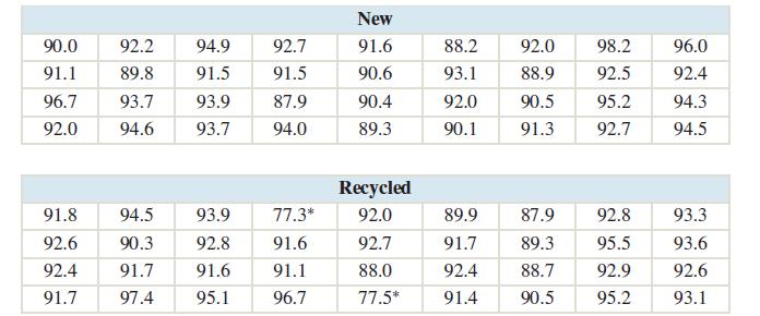
In a study described in the book Statistical Case Studies for Industrial Process Improvement by V. Czitrom and P. Spagon, both new and recycled wafers were oxidized, and the thicknesses of the layers were measured to determine whether they tended to differ between the two types of wafers. Recycled wafers are cheaper than new wafers, so the hope was that they would perform at least as well as the new wafers. Following are 36 thickness measurements (in tenths of a nanometer) for both new and recycled wafers.
1. Construct comparative boxplots for the thicknesses of new wafers and recycled wafers.
2. Identify all outliers.
3. Should any of the outliers be deleted? If so, delete them and redraw the boxplots.
4. Identify any outliers in the redrawn boxplots. Should any of these be deleted? Explain.
5. Are the distributions of thicknesses skewed, or approximately symmetric?
6. Delete outliers as appropriate, and compute the mean thickness for new and for recycled wafers.
7. Delete outliers as appropriate, and compute the median thickness for new and for recycled wafers.
8. Delete outliers as appropriate, and compute the standard deviation of the thicknesses for new and for recycled wafers.
9. Suppose that it is desired to use the type of wafer whose distribution has less spread. Write a brief paragraph that explains which type of wafer to use and why. Which measure is more useful for spread in this case, the standard deviation or the interquartile range? Explain.
Step by Step Answer:


