Answered step by step
Verified Expert Solution
Question
1 Approved Answer
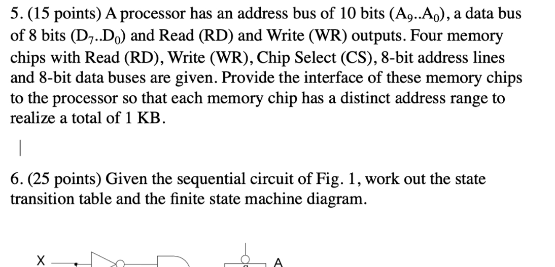
( 1 5 points ) A processor has an address bus of 1 0 bits ( A 9 . . A 0 ) , a
points A processor has an address bus of bits a data bus
of bits and Read RD and Write WR outputs. Four memory
chips with Read RD Write WR Chip Select CSbit address lines
and bit data buses are given. Provide the interface of these memory chips
to the processor so that each memory chip has a distinct address range to
realize a total of
points Given the sequential circuit of Fig. work out the state
transition table and the finite state machine diagram.

Step by Step Solution
There are 3 Steps involved in it
Step: 1

Get Instant Access to Expert-Tailored Solutions
See step-by-step solutions with expert insights and AI powered tools for academic success
Step: 2

Step: 3

Ace Your Homework with AI
Get the answers you need in no time with our AI-driven, step-by-step assistance
Get Started


