Answered step by step
Verified Expert Solution
Question
1 Approved Answer
1. (5 points) Sketch an equivalent NAND-BOR realization of the AND-OR circuit of Figure 1. The circuit realizes the MSOP expression F = 7 .W
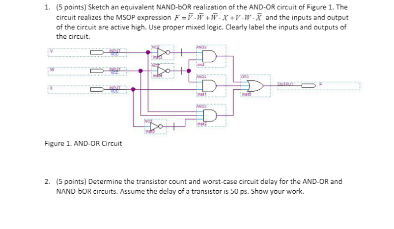
1. (5 points) Sketch an equivalent NAND-BOR realization of the AND-OR circuit of Figure 1. The circuit realizes the MSOP expression F = 7 .W +X +V.W - X and the inputs and output of the circuit are active high. Use proper mixed logic. Clearly label the inputs and outputs of the circuit AND2 ANDS inst Figure 1. AND-OR Circuit 2. (5 points) Determine the transistor count and worst-case circuit delay for the AND-OR and NAND-BOR circuits. Assume the delay of a transistor is 50 ps. Show your work. 1. (5 points) Sketch an equivalent NAND-BOR realization of the AND-OR circuit of Figure 1. The circuit realizes the MSOP expression F = 7 .W +X +V.W - X and the inputs and output of the circuit are active high. Use proper mixed logic. Clearly label the inputs and outputs of the circuit AND2 ANDS inst Figure 1. AND-OR Circuit 2. (5 points) Determine the transistor count and worst-case circuit delay for the AND-OR and NAND-BOR circuits. Assume the delay of a transistor is 50 ps. Show your work
Step by Step Solution
There are 3 Steps involved in it
Step: 1
Get Instant Access to Expert-Tailored Solutions
See step-by-step solutions with expert insights and AI powered tools for academic success
Step: 2
Step: 3
Ace Your Homework with AI
Get the answers you need in no time with our AI-driven, step-by-step assistance
Get Started