

Answered step by step
Verified Expert Solution
Question
1 Approved Answer
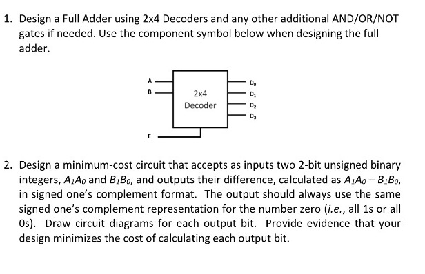
1. Design a Full Adder using 2x4 Decoders and any other additional AND/OR/NOT gates if needed. Use the component symbol below when designing the full
Step by Step Solution
There are 3 Steps involved in it
Step: 1

Get Instant Access to Expert-Tailored Solutions
See step-by-step solutions with expert insights and AI powered tools for academic success
Step: 2

Step: 3
Ace Your Homework with AI
Get the answers you need in no time with our AI-driven, step-by-step assistance
Get Started
Concepts of Database Management
Authors: Philip J. Pratt, Mary Z. Last
8th edition
1285427106, 978-1285427102