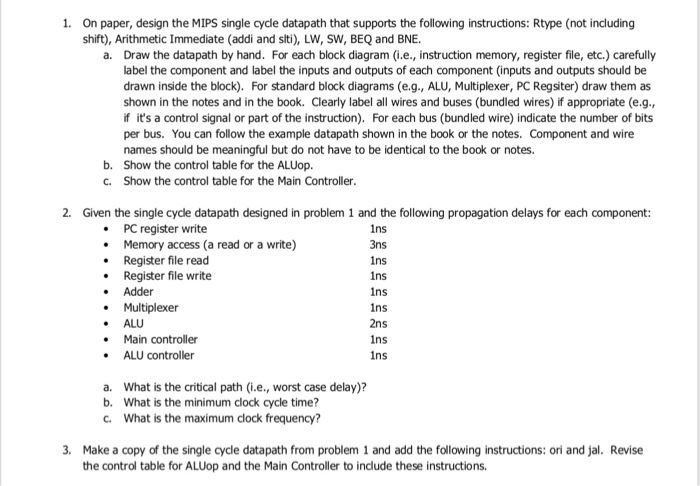
1. On paper, design the MIPS single cycle datapath that supports the following instructions: Rtype (not including shift), Arithmetic Immediate (addi and slti), LW, SW, BEQ and BNE. a. Draw the datapath by hand. For each block diagram (i.e., instruction memory, register file, etc.) carefully label the component and label the inputs and outputs of each component (inputs and outputs should be drawn inside the block). For standard block diagrams (e.g., ALU, Multiplexer, PC Regsiter) draw them as shown in the notes and in the book. Clearly label all wires and buses (bundled wires) if appropriate (e.g if it's a control signal or part of the instruction). For each bus (bundled wire) indicate the number of bits per bus. You can follow the example datapath shown in the book or the notes. Component and wire names should be meaningful but do not have to be identical to the book or notes. Show the control table for the ALUop Show the control table for the Main Controller b. C. 2. Given the single cycle datapath designed in problem 1 and the following propagation delays for each component: .PC register write . Memory access (a read or a write) .Register file read . Register file write Ins 3ns Ins Ins Ins Ins Adder . Multiplexer ALU Main controller ALU controller Ins Ins a. What is the critical path (.e., worst case delay)? b. What is the minimum clock cycle time? C. What is the maximum clock frequency 3. Make a copy of the single cycle datapath from problem 1 and add the following instructions: ori and jal. Revise the control table for ALUop and the Main Controller to include these instructions. 1. On paper, design the MIPS single cycle datapath that supports the following instructions: Rtype (not including shift), Arithmetic Immediate (addi and slti), LW, SW, BEQ and BNE. a. Draw the datapath by hand. For each block diagram (i.e., instruction memory, register file, etc.) carefully label the component and label the inputs and outputs of each component (inputs and outputs should be drawn inside the block). For standard block diagrams (e.g., ALU, Multiplexer, PC Regsiter) draw them as shown in the notes and in the book. Clearly label all wires and buses (bundled wires) if appropriate (e.g if it's a control signal or part of the instruction). For each bus (bundled wire) indicate the number of bits per bus. You can follow the example datapath shown in the book or the notes. Component and wire names should be meaningful but do not have to be identical to the book or notes. Show the control table for the ALUop Show the control table for the Main Controller b. C. 2. Given the single cycle datapath designed in problem 1 and the following propagation delays for each component: .PC register write . Memory access (a read or a write) .Register file read . Register file write Ins 3ns Ins Ins Ins Ins Adder . Multiplexer ALU Main controller ALU controller Ins Ins a. What is the critical path (.e., worst case delay)? b. What is the minimum clock cycle time? C. What is the maximum clock frequency 3. Make a copy of the single cycle datapath from problem 1 and add the following instructions: ori and jal. Revise the control table for ALUop and the Main Controller to include these instructions


