1. You will design a multiplication circuit which has 2 inputs : 5 bit multiplicand (binary) and 5 bit multiplier(binary). The circuit should apply the following multiplication rules: Multiply the multiplicand by two 'k' times, here 'k' is the maximum value that still allows to determine the result by using sum opertion. Then add multiplicand 'r' times to the multiplicand*2\) to determine the result. Here Y' is (multiplier - 24). See the examples below. E.g.1: 24x12 = 24*2*2*2 + (24 +24+24 +24) = 288 E.g.2: 31x22 = 31*2*2*2*2 + (31+31+31+31+31+31) = 682 a. Design the circuit and explain the design principles detailed enough. The design must include a moore type finite state machine and the required peripherals. b. Plot your circuit using the blocks, give the structure of each block using and/orot Gates. 2. Design an Algorithmic state machine (ASM) that adds 'n' consequtive values inside RAM space from address
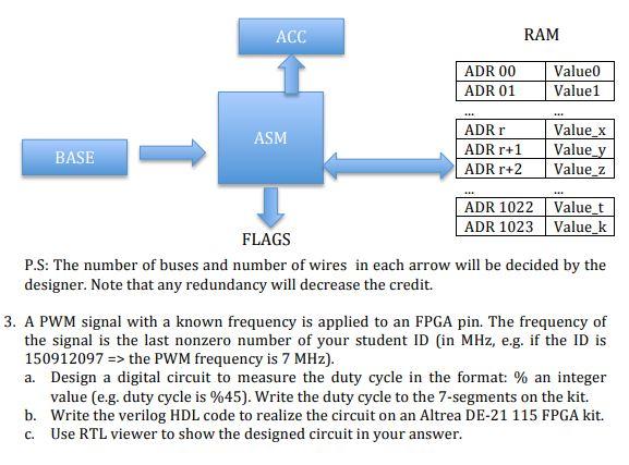
to address
. The values are changing between zero and 63 and the result should be stored in ACCUMULATOR register. The address
will be read from the register BASE by the ASM. Value 'n' is given as five times the last non-zero number of your student ID (if the ID is 15091209 7 => n=7*5 = 35 times). ACC RAM ADR 00 ADR 01 Value Value1 ASM BASE ADR r ADR r+1 ADR r+2 Value x Value_y Value_z ADR 1022 Value_t ADR 1023 Value_k FLAGS P.S: The number of buses and number of wires in each arrow will be decided by the designer. Note that any redundancy will decrease the credit. 3. A PWM signal with a known frequency is applied to an FPGA pin. The frequency of the signal is the last nonzero number of your student ID in MHz, e.g. if the ID is 150912097 => the PWM frequency is 7 MHz). a. Design a digital circuit to measure the duty cycle in the format: % an integer value (e.g. duty cycle is %45). Write the duty cycle to the 7-segments on the kit. b. Write the verilog HDL code to realize the circuit on an Altrea DE-21 115 FPGA kit. Use RTL viewer to show the designed circuit in your answer. C. 1. You will design a multiplication circuit which has 2 inputs : 5 bit multiplicand (binary) and 5 bit multiplier(binary). The circuit should apply the following multiplication rules: Multiply the multiplicand by two 'k' times, here 'k' is the maximum value that still allows to determine the result by using sum opertion. Then add multiplicand 'r' times to the multiplicand*2\) to determine the result. Here Y' is (multiplier - 24). See the examples below. E.g.1: 24x12 = 24*2*2*2 + (24 +24+24 +24) = 288 E.g.2: 31x22 = 31*2*2*2*2 + (31+31+31+31+31+31) = 682 a. Design the circuit and explain the design principles detailed enough. The design must include a moore type finite state machine and the required peripherals. b. Plot your circuit using the blocks, give the structure of each block using and/orot Gates. 2. Design an Algorithmic state machine (ASM) that adds 'n' consequtive values inside RAM space from address
to address
. The values are changing between zero and 63 and the result should be stored in ACCUMULATOR register. The address
will be read from the register BASE by the ASM. Value 'n' is given as five times the last non-zero number of your student ID (if the ID is 15091209 7 => n=7*5 = 35 times). ACC RAM ADR 00 ADR 01 Value Value1 ASM BASE ADR r ADR r+1 ADR r+2 Value x Value_y Value_z ADR 1022 Value_t ADR 1023 Value_k FLAGS P.S: The number of buses and number of wires in each arrow will be decided by the designer. Note that any redundancy will decrease the credit. 3. A PWM signal with a known frequency is applied to an FPGA pin. The frequency of the signal is the last nonzero number of your student ID in MHz, e.g. if the ID is 150912097 => the PWM frequency is 7 MHz). a. Design a digital circuit to measure the duty cycle in the format: % an integer value (e.g. duty cycle is %45). Write the duty cycle to the 7-segments on the kit. b. Write the verilog HDL code to realize the circuit on an Altrea DE-21 115 FPGA kit. Use RTL viewer to show the designed circuit in your answer. C