

Question
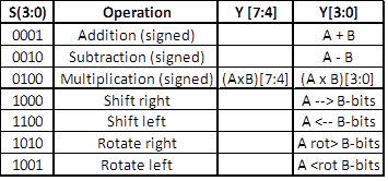
1.Design an ALU circuit that will use the instructions listed in Table 1 on the S bus. The input numbers A and B are signed,
1.Design an ALU circuit that will use the instructions listed in Table 1 on the S bus. The input numbers A and B are signed, 4-bit values (A[3] and B[3] are the sign bits). Note that only the arithmetic operations (+, -, *) are signed and the multiplication operation has an 8-bit product. The ALU must be implemented using Verilog code within the Xilinx WebPack IDE.
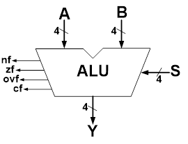
Modify the ALU designed in problem 1 to include several flag bits that will be set/cleared according to the ALU operation results. The complete ALU circuit is shown in Figure 1. The carry flag (cf) is set when an output carry exists, the overflow flag (ovf) is set when an overflow occurs, the zero flag (zf) is set when the output is 4b0000, and the negative flag (nf) is set when the sign bit y[3] is 1.
Develop a Verilog testbench to validate the designed ALU and implement it using Xilinx WebPack. Include the testbench code and associated results for full credit.
S (3:0) Operation Y [7:4] Y13:01 0001 Addition (signed) A B A-B 0010 Subtraction (signed 0100 Multi cation (signed) AxB)(7:4] (A x B) 3:0 1000 Shift right A B-bits 1100 Shift left A B-bits 1010 Rotate right A rot B-bits 1001 Rotate left A Krot B-bits S (3:0) Operation Y [7:4] Y13:01 0001 Addition (signed) A B A-B 0010 Subtraction (signed 0100 Multi cation (signed) AxB)(7:4] (A x B) 3:0 1000 Shift right A B-bits 1100 Shift left A B-bits 1010 Rotate right A rot B-bits 1001 Rotate left A Krot B-bitsStep by Step Solution
There are 3 Steps involved in it
Step: 1

Get Instant Access to Expert-Tailored Solutions
See step-by-step solutions with expert insights and AI powered tools for academic success
Step: 2

Step: 3
Ace Your Homework with AI
Get the answers you need in no time with our AI-driven, step-by-step assistance
Get Started
Relational Database Technology
Authors: Suad Alagic
1st Edition
354096276X, 978-3540962762