Answered step by step
Verified Expert Solution
Link Copied!

Question

1 Approved Answer

3. (12 points) Realize the MSOP Boolean expression F=VW~+VWX (sketch the circuit) using SSI NAND and NOT gates (NAND-bOR circuit). The circuit inputs and outputs
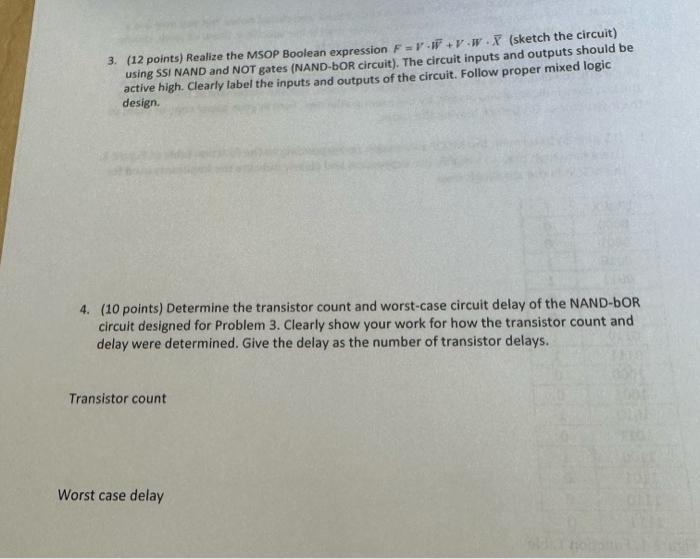
image text in transcribed
3. (12 points) Realize the MSOP Boolean expression F=VW~+VWX (sketch the circuit) using SSI NAND and NOT gates (NAND-bOR circuit). The circuit inputs and outputs should be active high. Clearly label the inputs and outputs of the circuit. Follow proper mixed logic design. 4. (10 points) Determine the transistor count and worst-case circuit delay of the NAND-bOR circuit designed for Problem 3 . Clearly show your work for how the transistor count and delay were determined. Give the delay as the number of transistor delays. Transistor count Worst case delay

Step by Step Solution

There are 3 Steps involved in it

Step: 1

blur-text-image

Get Instant Access to Expert-Tailored Solutions

See step-by-step solutions with expert insights and AI powered tools for academic success

Step: 2

blur-text-image

Step: 3

blur-text-image

Ace Your Homework with AI

Get the answers you need in no time with our AI-driven, step-by-step assistance

Get Started

Recommended Textbook for

Accounting And Auditing Research And Databases Practitioner's Desk Reference

Authors: Thomas R. Weirich, Natalie Tatiana Churyk, Thomas C. Pearson

1st Edition

1118334426, 978-1118334423

More Books

Students also viewed these Databases questions

Question

What is Change Control and how does it operate?

Answered: 1 week ago

Question

How do Data Requirements relate to Functional Requirements?

Answered: 1 week ago