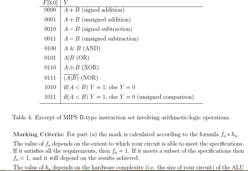

3. (14 marks) In this assignment you will design an arithmetic logic unit (ALU) which can be used readily in a MIPS processor. In particular, we focus on the arithmetic logic instructions among MIPS R-type instructions. Each machine instruction in a MIPS processor has a 6 bit field called "Funct" (denoted briefly by F here). A MIPS compatible ALU takes F3:0 as a control input. This control input determines the relation between the data inputs A and B, and the output Y as per Table 4, which is a part of the set of MIPS R-type instructions. A step by step design process is described in the lecture slides. Note that the ALU hardware includes an adder. For this assignment you are free to choose any adder implementation including the behavioural one using System Verilog+ operator. . (8 marks) Design an n bit wide parameterized ALU module as per Table 4. The ALU should have two additional outputs Cout and OV to flag the carry out and arithmetic overflow in arithmetic operations (6 marks) Design an appropriate test-bench to simulate the functionality of your de- signed circuit on some simulator like Modelsim 3. (14 marks) In this assignment you will design an arithmetic logic unit (ALU) which can be used readily in a MIPS processor. In particular, we focus on the arithmetic logic instructions among MIPS R-type instructions. Each machine instruction in a MIPS processor has a 6 bit field called "Funct" (denoted briefly by F here). A MIPS compatible ALU takes F3:0 as a control input. This control input determines the relation between the data inputs A and B, and the output Y as per Table 4, which is a part of the set of MIPS R-type instructions. A step by step design process is described in the lecture slides. Note that the ALU hardware includes an adder. For this assignment you are free to choose any adder implementation including the behavioural one using System Verilog+ operator. . (8 marks) Design an n bit wide parameterized ALU module as per Table 4. The ALU should have two additional outputs Cout and OV to flag the carry out and arithmetic overflow in arithmetic operations (6 marks) Design an appropriate test-bench to simulate the functionality of your de- signed circuit on some simulator like Modelsim


