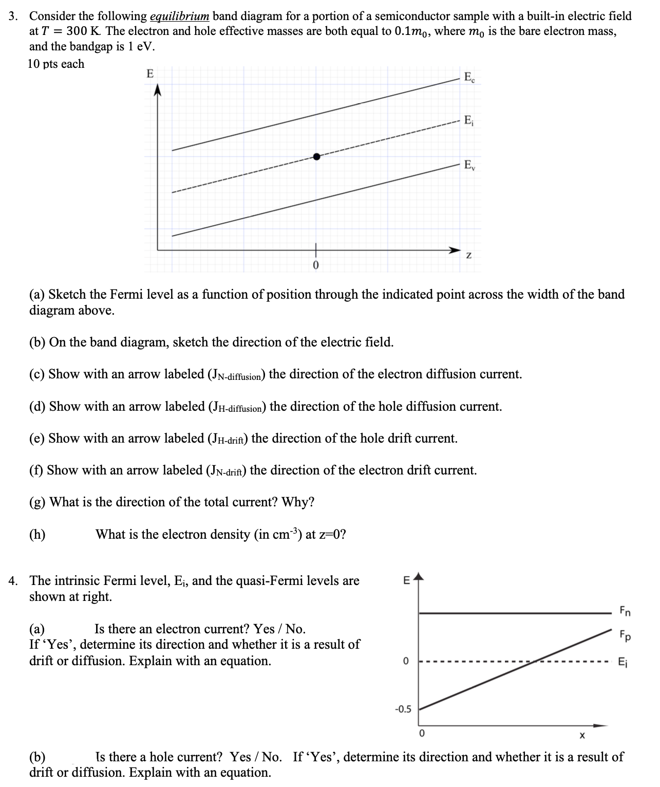
3. Consider the following equilibrium band diagram for a portion of a semiconductor sample with a built-in electric field at T = 300 K.

3. Consider the following equilibrium band diagram for a portion of a semiconductor sample with a built-in electric field at T = 300 K. The electron and hole effective masses are both equal to 0.1mo, where mo is the bare electron mass, and the bandgap is 1 eV. 10 pts each E 0 E Ev Z (a) Sketch the Fermi level as a function of position through the indicated point across the width of the band diagram above. (b) On the band diagram, sketch the direction of the electric field. (c) Show with an arrow labeled (JN-diffusion) the direction of the electron diffusion current. (d) Show with an arrow labeled (JH-diffusion) the direction of the hole diffusion current. (e) Show with an arrow labeled (JH-drift) the direction of the hole drift current. (f) Show with an arrow labeled (JN-drift) the direction of the electron drift current. (g) What is the direction of the total current? Why? (h) What is the electron density (in cm) at z=0? 4. The intrinsic Fermi level, Ei, and the quasi-Fermi levels are shown at right. (a) Is there an electron current? Yes / No. If 'Yes', determine its direction and whether it is a result of drift or diffusion. Explain with an equation. E Fn 0 Ei -0.5 0 X (b) Is there a hole current? Yes/No. If 'Yes', determine its direction and whether it is a result of drift or diffusion. Explain with an equation.
Step by Step Solution
There are 3 Steps involved in it
Step: 1
To answer these questions lets break them down stepbystep based on the provided band diagram and information 3a Sketch the Fermi level as a function of position through the indicated point across the ...
See step-by-step solutions with expert insights and AI powered tools for academic success
Step: 2

Step: 3

Ace Your Homework with AI
Get the answers you need in no time with our AI-driven, step-by-step assistance
Get Started


