Question
3) Design of a switching power converter PART I. Power electronic circuits depend on digital design for their control. A boost converter is one example,
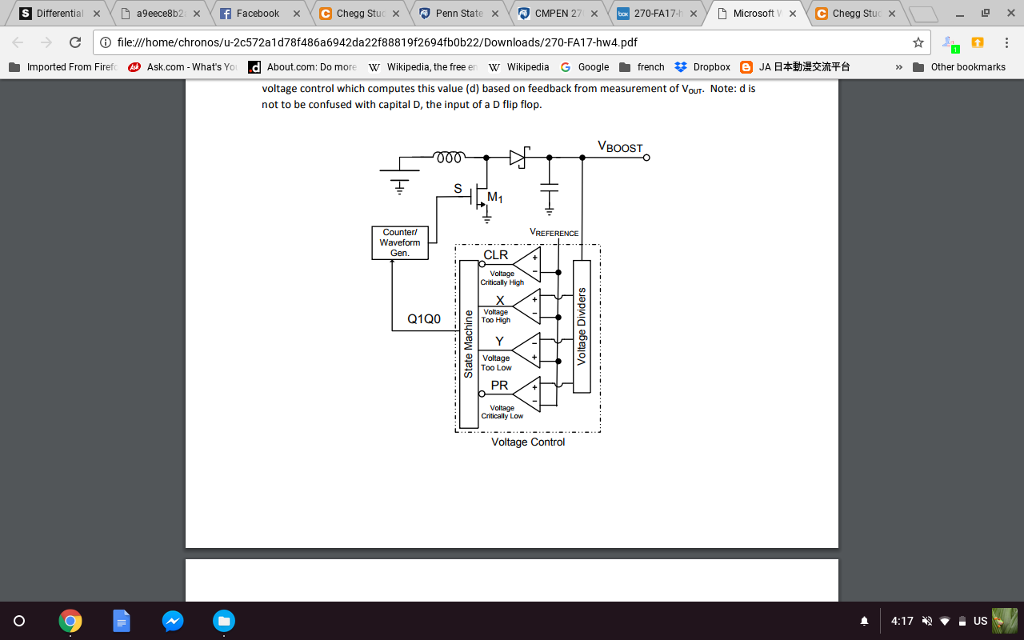
3) Design of a switching power converter PART I. Power electronic circuits depend on digital design for their control. A boost converter is one example, where its switching control input (S) to its NMOS transistor is a square wave of variable duty cycle (d), and ideal voltage gain of 1/(1-d), i.e. VOUT = VIN/(1- d). This charges up an inductor d % of the time, and then dumps the charge through a diode onto an output capacitor during each off cycle the result is a boosted voltage. You can use these for many interesting projects converting small voltages, i.e. from a battery or solar cell to power heavy loads like motors, bright lights, transmitters, etc. If VIN is fixed (i.e. from a battery) what happens to VOUT as we increase the duty cycle towards 100%? AKA dont try this @ home. NOT a graded question just something to think about! The following is a schematic of a DC/DC boost converter CMOS chip for a medical implantable device application. The circuit works by converting its small input voltage of 0.8 V max to 2 V (VOUT) so that a CMOS transmitter has enough voltage to reliably output a wireless signal from an implant under the animals skin. Although the ideal voltage gain equation helps estimate the output voltage, circuit conditions such as losses from the NMOS, inductor, diode, as well as an unreliable input voltage all influence the actual duty cycle necessary to provide the 2 V output. Part I of this activity is to design the voltage control which computes this value (d) based on feedback from measurement of VOUT. Note: d is not to be confused with capital D, the input of a D flip flop.

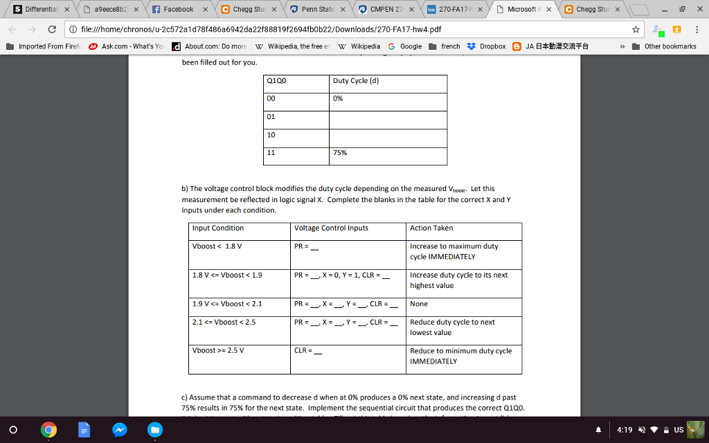
a) We designate Q1Q0 to be the state variables representing the duty cycle of the square wave activating NMOS switch M1. Note that operating at exactly 100% duty cycle would mean S = 1 constantly and short the inductor to ground, which wouldnt allow any charge transfer to VOUT, and will probably cook the inductor! However, zero percent is useful because when S = 0 the system will turn off completely to save power when not in use. Find all values (in equally spaced intervals from 0% - 75%) that can be realized with the 2-bit scheme. Record this in a table that lists the states to the corresponding duty cycle. Q1Q0 = 00, Q1Q0 = 11 have been filled out for you.

c) Assume that a command to decrease d when at 0% produces a 0% next state, and increasing d past 75% results in 75% for the next state. Implement the sequential circuit that produces the correct Q1Q0. It is best to start with a state transition table. Fill out this table based on the information in part (b). d) Draw the state machine diagram corresponding to the table from part (c) e) Design and draw the circuit based on the information from parts (c) and (d) f) Notice in your circuit design that the inclusion of the PR and CLR conditions are asynchronous. Why was this preferred instead of synchronizing with the clock like X and Y? d) Draw the state machine diagram corresponding to the table from part (c)
PLEASE ANSWER THE WHOLE QUESTION!! THANK YOU!!
Differential Y D a9eece8b2 x. R Facebook (eChegg Stu \Penn StatXCMPEN 2/X 270-FA1 71 y D Microsoft /XYeChegg Stu C file://home/chronos/u-2c572a1d78f486a6942da22f88819f2694fb0b22/Downloads/270-FA17-hw4.pdf -Imported From FirefAsk.com what's Y E About.com : Domor W Wikipedia, the free e W Wikipedia G Google-french ; Dropbox JA Other bookmarks voltage control which computes this value (d) based on feedback from measurement of VouT. Note: d is not to be confused with capital D, the input of a D flip flop. VBoOST VREFERENCE Waveform Gen CLR Critically High Q10o o Votage Too High oltage Too Low PR+ Criticaly Low Voltage Control 4:17 US Differential Y D a9eece8b2 x. R Facebook (eChegg Stu \Penn StatXCMPEN 2/X 270-FA1 71 y D Microsoft /XYeChegg Stu C file://home/chronos/u-2c572a1d78f486a6942da22f88819f2694fb0b22/Downloads/270-FA17-hw4.pdf -Imported From FirefAsk.com what's Y E About.com : Domor W Wikipedia, the free e W Wikipedia G Google-french ; Dropbox JA Other bookmarks voltage control which computes this value (d) based on feedback from measurement of VouT. Note: d is not to be confused with capital D, the input of a D flip flop. VBoOST VREFERENCE Waveform Gen CLR Critically High Q10o o Votage Too High oltage Too Low PR+ Criticaly Low Voltage Control 4:17 US
Step by Step Solution
There are 3 Steps involved in it
Step: 1

Get Instant Access to Expert-Tailored Solutions
See step-by-step solutions with expert insights and AI powered tools for academic success
Step: 2

Step: 3

Ace Your Homework with AI
Get the answers you need in no time with our AI-driven, step-by-step assistance
Get Started


