Answered step by step
Verified Expert Solution
Link Copied!

Question

1 Approved Answer

4 points) For the following Verilog description of a 2-input NAND gate, the input signal is switched from Al,B to (Al,B 10, please tell the
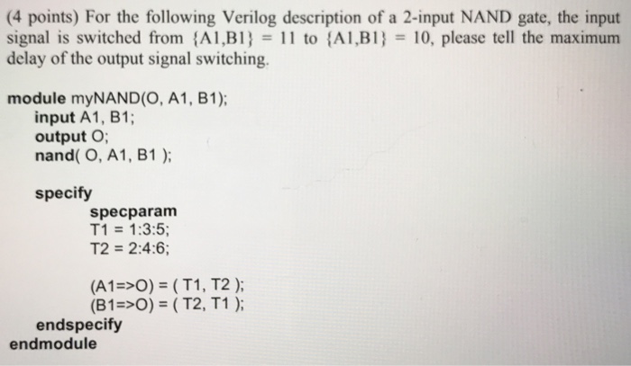
image text in transcribed
4 points) For the following Verilog description of a 2-input NAND gate, the input signal is switched from Al,B to (Al,B 10, please tell the maximum delay of the output signal switching. module myNAND(O, A1, B1) input A1, B1; output O; nand( O, A1, B1 ); specify specparam T1 1:3:5 T2 = 2:46; (A1 >o) (T1, T2 ); (BI=>O) = ( T2, T1 ); endspecify endmodule

Step by Step Solution

There are 3 Steps involved in it

Step: 1

blur-text-image

Get Instant Access to Expert-Tailored Solutions

See step-by-step solutions with expert insights and AI powered tools for academic success

Step: 2

blur-text-image

Step: 3

blur-text-image

Ace Your Homework with AI

Get the answers you need in no time with our AI-driven, step-by-step assistance

Get Started

Recommended Textbook for

Database Concepts International Edition

Authors: David M. Kroenke

6th Edition International Edition

0133098222, 978-0133098228

More Books

Students also viewed these Databases questions