

Question: 7.1 Objective In the final project, you are required to design and implement a 4-bit Booth's Multiplier, which performs the multiplication of two signed binary
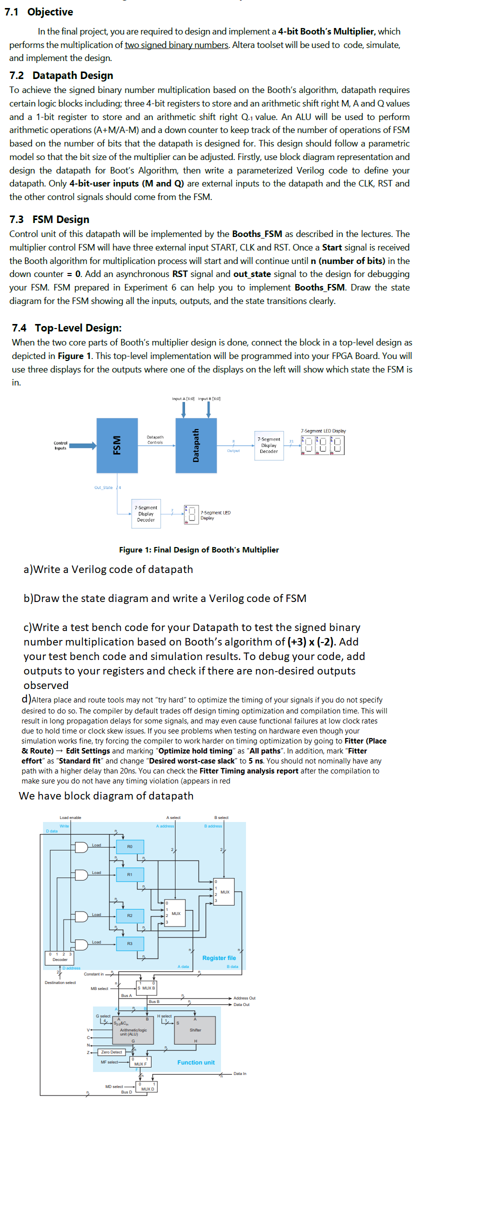
7.1 Objective In the final project, you are required to design and implement a 4-bit Booth's Multiplier, which performs the multiplication of two signed binary numbers. Altera toolset will be used to code, simulate, and implement the design. 7.2 Datapath Design To achieve the signed binary number multiplication based on the Booth's algorithm, datapath requires certain logic blocks including; three 4-bit registers to store and an arithmetic shift right M, A and Q values and a 1-bit register to store and an arithmetic shift right Q.1 value. An ALU will be used to perform arithmetic operations (A+M/A-M) and a down counter to keep track of the number of operations of FSM based on the number of bits that the datapath is designed for. This design should follow a parametric model so that the bit size of the multiplier can be adjusted. Firstly, use block diagram representation and design the datapath for Boot's Algorithm, then write a parameterized Verilog code to define your datapath. Only 4-bit-user inputs (M and Q) are external inputs to the datapath and the CLK, RST and the other control signals should come from the FSM. 7.3 FSM Design Control unit of this datapath will be implemented by the Booths_FSM as described in the lectures. The multiplier control FSM will have three external input START, CLK and RST. Once a Start signal is received the Booth algorithm for multiplication process will start and will continue until n (number of bits) in the down counter = 0. Add an asynchronous RST signal and out_state signal to the design for debugging your FSM. FSM prepared in Experiment 6 can help you to implement Booths_FSM. Draw the state diagram for the FSM showing all the inputs, outputs, and the state transitions clearly. 7.4 Top-Level Design: When the two core parts of Booth's multiplier design is done, connect the block in a top-level design as depicted in Figure 1. This top-level implementation will be programmed into your FPGA Board. You will use three displays for the outputs where one of the displays on the left will show which state the FSM is in. Input A [3:0 Input B (3:0) 7-Segment LED Display Datapath Controls 21 Control Inputs FSM Datapath 7-Segment Display Decoder 1018 Dutput Out_State 4 7-Segment Display Decoder 7-Segment LED U Display Figure 1: Final Design of Booth's Multiplier a)Write a Verilog code of datapath b)Draw the state diagram and write a Verilog code of FSM c)Write a test bench code for your Datapath to test the signed binary number multiplication based on Booth's algorithm of (+3) (-2). Add your test bench code and simulation results. To debug your code, add outputs to your registers and check if there are non-desired outputs observed d)Altera place and route tools may not "try hard" to optimize the timing of your signals if you do not specify desired to do so. The compiler by default trades off design timing optimization and compilation time. This will result in long propagation delays for some signals, and may even cause functional failures at low clock rates due to hold time or clock skew issues. If you see problems when testing on hardware even though your simulation works fine, try forcing the compiler to work harder on timing optimization by going to Fitter (Place & Route) + Edit Settings and marking "Optimize hold timing" as "All paths. In addition, mark "Fitter effort" as "Standard fit" and change "Desired worst-case slack" to 5 ns. You should not nominally have any path with a higher delay than 20ns. You can check the Fitter Timing analysis report after the compilation to make sure you do not have any timing violation (appears in red We have block diagram of datapath Load enable A select B select Baddress Write D data Load RO Load RI Load MUX R2 Load R3 Decoder Register file B data Daddress Constantin Destination select MB select ny 11 S MUXB Bus A Address Out Data Out Geld H select $208c Arithmetic logic Shifter unit (ALU) H Zero Detect MF select MUX Function unit Data in MD select Bus MUXD 7.1 Objective In the final project, you are required to design and implement a 4-bit Booth's Multiplier, which performs the multiplication of two signed binary numbers. Altera toolset will be used to code, simulate, and implement the design. 7.2 Datapath Design To achieve the signed binary number multiplication based on the Booth's algorithm, datapath requires certain logic blocks including; three 4-bit registers to store and an arithmetic shift right M, A and Q values and a 1-bit register to store and an arithmetic shift right Q.1 value. An ALU will be used to perform arithmetic operations (A+M/A-M) and a down counter to keep track of the number of operations of FSM based on the number of bits that the datapath is designed for. This design should follow a parametric model so that the bit size of the multiplier can be adjusted. Firstly, use block diagram representation and design the datapath for Boot's Algorithm, then write a parameterized Verilog code to define your datapath. Only 4-bit-user inputs (M and Q) are external inputs to the datapath and the CLK, RST and the other control signals should come from the FSM. 7.3 FSM Design Control unit of this datapath will be implemented by the Booths_FSM as described in the lectures. The multiplier control FSM will have three external input START, CLK and RST. Once a Start signal is received the Booth algorithm for multiplication process will start and will continue until n (number of bits) in the down counter = 0. Add an asynchronous RST signal and out_state signal to the design for debugging your FSM. FSM prepared in Experiment 6 can help you to implement Booths_FSM. Draw the state diagram for the FSM showing all the inputs, outputs, and the state transitions clearly. 7.4 Top-Level Design: When the two core parts of Booth's multiplier design is done, connect the block in a top-level design as depicted in Figure 1. This top-level implementation will be programmed into your FPGA Board. You will use three displays for the outputs where one of the displays on the left will show which state the FSM is in. Input A [3:0 Input B (3:0) 7-Segment LED Display Datapath Controls 21 Control Inputs FSM Datapath 7-Segment Display Decoder 1018 Dutput Out_State 4 7-Segment Display Decoder 7-Segment LED U Display Figure 1: Final Design of Booth's Multiplier a)Write a Verilog code of datapath b)Draw the state diagram and write a Verilog code of FSM c)Write a test bench code for your Datapath to test the signed binary number multiplication based on Booth's algorithm of (+3) (-2). Add your test bench code and simulation results. To debug your code, add outputs to your registers and check if there are non-desired outputs observed d)Altera place and route tools may not "try hard" to optimize the timing of your signals if you do not specify desired to do so. The compiler by default trades off design timing optimization and compilation time. This will result in long propagation delays for some signals, and may even cause functional failures at low clock rates due to hold time or clock skew issues. If you see problems when testing on hardware even though your simulation works fine, try forcing the compiler to work harder on timing optimization by going to Fitter (Place & Route) + Edit Settings and marking "Optimize hold timing" as "All paths. In addition, mark "Fitter effort" as "Standard fit" and change "Desired worst-case slack" to 5 ns. You should not nominally have any path with a higher delay than 20ns. You can check the Fitter Timing analysis report after the compilation to make sure you do not have any timing violation (appears in red We have block diagram of datapath Load enable A select B select Baddress Write D data Load RO Load RI Load MUX R2 Load R3 Decoder Register file B data Daddress Constantin Destination select MB select ny 11 S MUXB Bus A Address Out Data Out Geld H select $208c Arithmetic logic Shifter unit (ALU) H Zero Detect MF select MUX Function unit Data in MD select Bus MUXD
Step by Step Solution
There are 3 Steps involved in it

Get step-by-step solutions from verified subject matter experts