Answered step by step
Verified Expert Solution
Question
1 Approved Answer
All the questions are part of one. Need a logic diagram, module, and testbench Build a register file with 32 32-bit registers with two write

All the questions are part of one. Need a logic diagram, module, and testbench
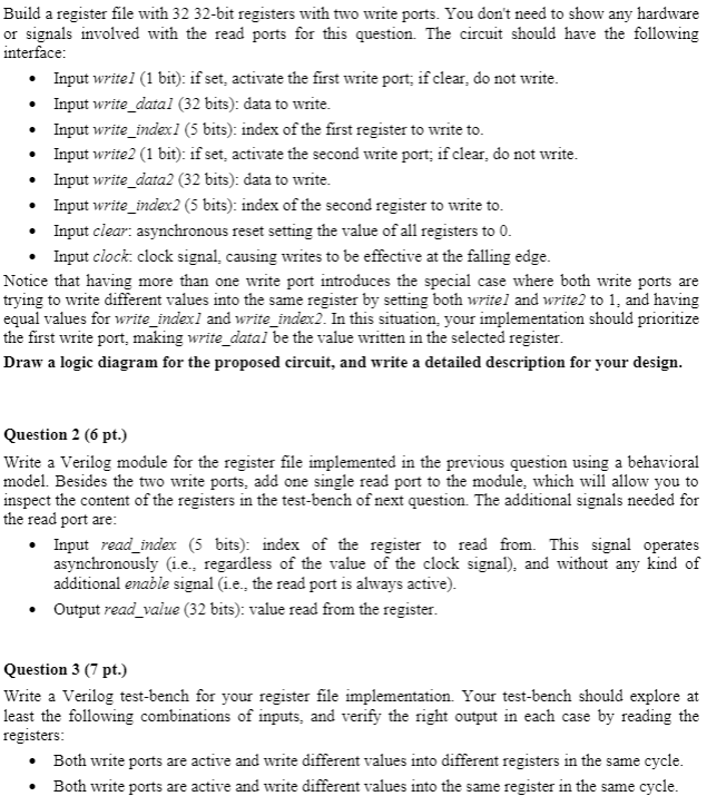
Build a register file with 32 32-bit registers with two write ports. You don't need to show any hardware or signals involved with the read ports for this question. The circuit should have the following interface: Input writel (1 bit): if set, activate the first write port, if clear, do not write. Input write_datal (32 bits): data to write. Input write_index1 (5 bits): index of the first register to write to. Input write2 (1 bit): if set activate the second write port, if clear, do not write. Input write_data2 (32 bits): data to write. Input write_index2 (5 bits): index of the second register to write to. Input clear. asynchronous reset setting the value of all registers to 0. Input clock clock signal, causing writes to be effective at the falling edge. Notice that having more than one write port introduces the special case where both write ports are trying to write different values into the same register by setting both writel and write2 to 1, and having equal values for write_indexl and write_index2. In this situation, your implementation should prioritize the first write port, making write_datal be the value written in the selected register. Draw a logic diagram for the proposed circuit, and write a detailed description for your design. Question 2 (6 pt.) Write a Verilog module for the register file implemented in the previous question using a behavioral model. Besides the two write ports, add one single read port to the module, which will allow you to inspect the content of the registers in the test-bench of next question. The additional signals needed for the read port are: Input read_index (5 bits): index of the register to read from. This signal operates asynchronously i.e. regardless of the value of the clock signal), and without any kind of additional enable signal (1.e. the read port is always active). Output read_value (32 bits): value read from the register. Question 3 (7 pt.) Write a Verilog test-bench for your register file implementation. Your test-bench should explore at least the following combinations of inputs, and verify the right output in each case by reading the registers: Both write ports are active and write different values into different registers in the same cycle. Both write ports are active and write different values into the same register in the same cycle. Build a register file with 32 32-bit registers with two write ports. You don't need to show any hardware or signals involved with the read ports for this question. The circuit should have the following interface: Input writel (1 bit): if set, activate the first write port, if clear, do not write. Input write_datal (32 bits): data to write. Input write_index1 (5 bits): index of the first register to write to. Input write2 (1 bit): if set activate the second write port, if clear, do not write. Input write_data2 (32 bits): data to write. Input write_index2 (5 bits): index of the second register to write to. Input clear. asynchronous reset setting the value of all registers to 0. Input clock clock signal, causing writes to be effective at the falling edge. Notice that having more than one write port introduces the special case where both write ports are trying to write different values into the same register by setting both writel and write2 to 1, and having equal values for write_indexl and write_index2. In this situation, your implementation should prioritize the first write port, making write_datal be the value written in the selected register. Draw a logic diagram for the proposed circuit, and write a detailed description for your design. Question 2 (6 pt.) Write a Verilog module for the register file implemented in the previous question using a behavioral model. Besides the two write ports, add one single read port to the module, which will allow you to inspect the content of the registers in the test-bench of next question. The additional signals needed for the read port are: Input read_index (5 bits): index of the register to read from. This signal operates asynchronously i.e. regardless of the value of the clock signal), and without any kind of additional enable signal (1.e. the read port is always active). Output read_value (32 bits): value read from the register. Question 3 (7 pt.) Write a Verilog test-bench for your register file implementation. Your test-bench should explore at least the following combinations of inputs, and verify the right output in each case by reading the registers: Both write ports are active and write different values into different registers in the same cycle. Both write ports are active and write different values into the same register in the same cycleStep by Step Solution
There are 3 Steps involved in it
Step: 1

Get Instant Access to Expert-Tailored Solutions
See step-by-step solutions with expert insights and AI powered tools for academic success
Step: 2

Step: 3

Ace Your Homework with AI
Get the answers you need in no time with our AI-driven, step-by-step assistance
Get Started


