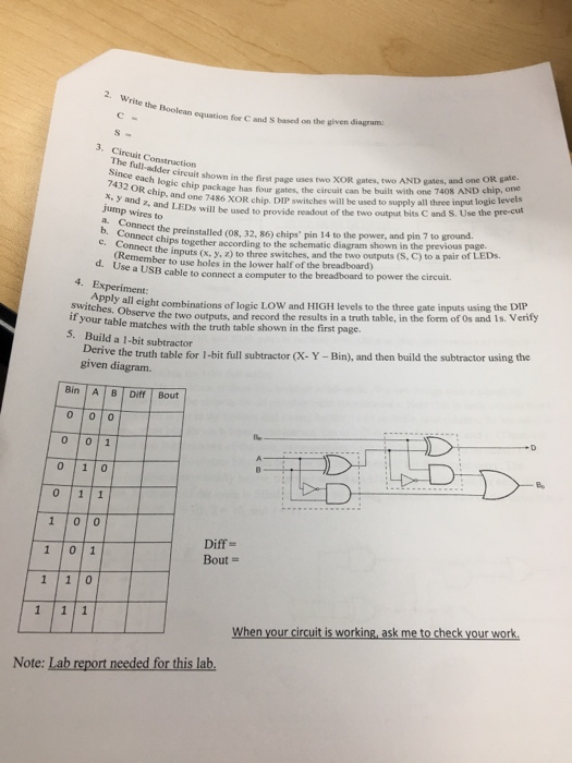
Computer science, complete answers will receive positive comment and thumbs up! Thank you
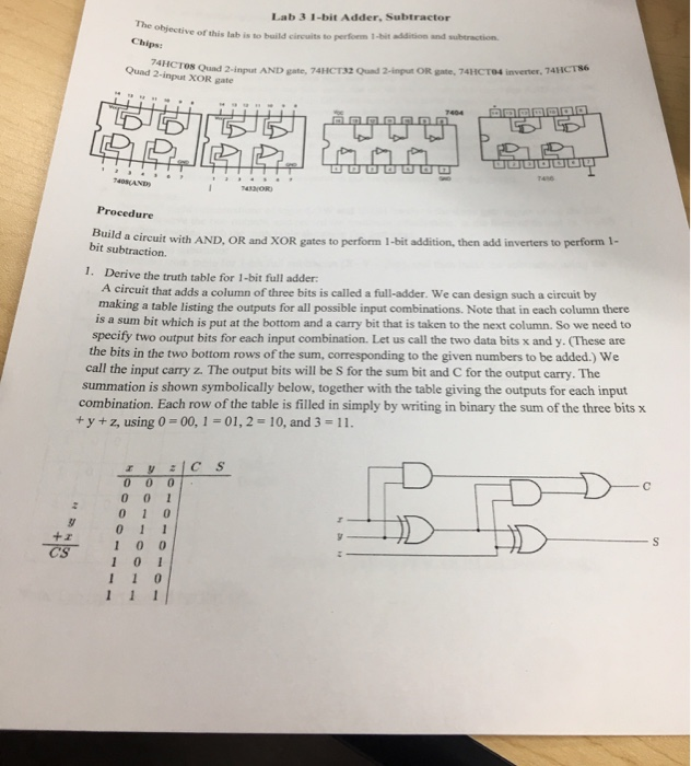
Lab 3 1-bit Adder, Subtractor of this lab is to build circuits to perfom 1-bit addition and subtraction uad Chips: Dund 2-input XOR gate S Quad 2-input AND gate, 74HCT32 Ound 2-input OR gate, 74HCT04 inverter, 741HCTS6 Procedure uild a circuit with AND, OR and XOR gates to perform 1-bit addition, then add inverters to perform 1- bit subtraction. 1. Derive the truth table for 1-bit full adder. A circuit that adds a column of three bits is called a full-adder. We can design such a circuit by making a table listing the outputs for all possible input combinations. Note that in each column there is a sum bit which is put at the bottom and a carry bit that is taken to the next column. So we need to specify two output bits for each input combination. Let us call the two data bits x and y. (These are the bits in the two bottom rows of the sum, corresponding to the given numbers to be added.) We call the input carry z. The output bits will be S for the sum bit and C for the output carry. The summation is shown symbolically below, together with the table giving the outputs for each input combination. Each row of the table is filled in simply by writing in binary the sum of the three bits x +y+ z, using 0 -00,1 01, 2 -10, and 3 1. 0 +2 0 11 2. Write the Boolean equation for ean equation for C and S based on the given diagram 3. Cireuit Construction Since each logic chip wdder ciruit shown in the first page uses two XOR gates, two AND gates, Ingrone 7486 xOR chip. DIP switches will be used to supply all three input logic levels 2 and LEDs will be used to provide readout of the two output bits C and S. Use the R chippackage has four gates, the circuit can be built with one 7408 AND chip, one x, y and z jump wires to a. Connect b. onecet the preinstalled (08, 32, 86) chips" pin 14 to the power, and pin 7 to ground. previous page. C,C chips together according to the schematic diagram shown in the inputs (x. y, z) to three switches, and the two outputs (S, C) to a pair of LEDs. emember to use holes in the lower half of the breadboard) cable to connect a computer to the breadboard to d. U se a USB ght combinations of logic LOW and HIGH levels to the three gate inputs using the DIP switches. Observe if your table 5. Build a 1-bit subtractor the two outputs, and record the results in a truth table, in the form of Os and 1s. Verify e matches with the truth table shown in the first page. ve the truth table for 1-bit full subtractor (X- Y - Bin), and then build the subtractor using the given diagram. Bin A B Diff Bout 0 0 1 0 1 0 1 00 1 0 1 1 1 0 Diff Bout- When your circuit is working, ask me to check your work Note: Lab report needed for this lab