Question
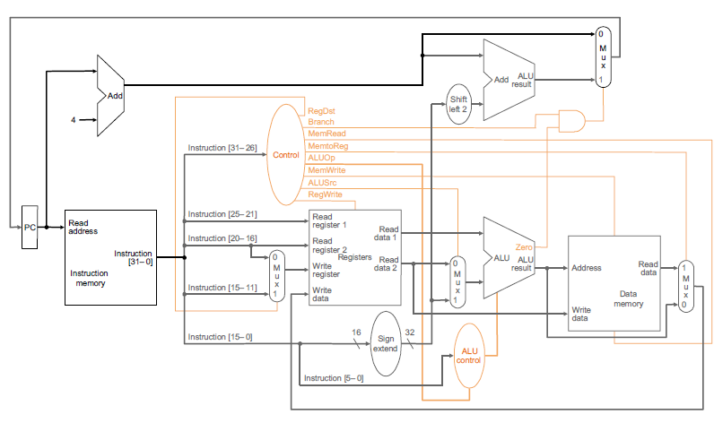
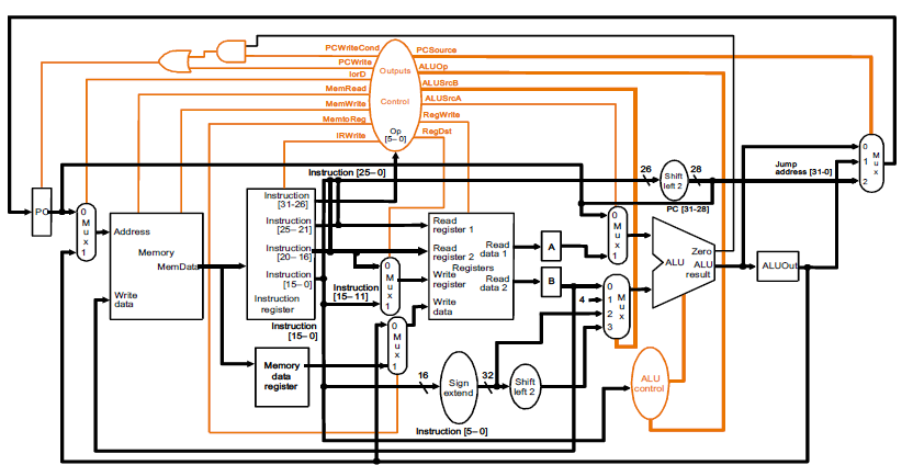
Consider the single cycle and multi-cycle implementations of the MIPS processor shown in the figures below. The time taken by each component in each of
Consider the single cycle and multi-cycle implementations of the MIPS processor shown in the figures below.


The time taken by each component in each of the two architectures is as follows: - Instruction Memory Access = 200 ps - Register File read from stable read-register number = 100 ps - ALU delay = 100 ps - Data Memory Access (read) = 300 ps - Write into registers / memory from rising edge of clock = 50 ps (where ps stands for pico-seconds (1 ps = 1 x 10-12 seconds)). The delays of multiplexers, control unit, shifters, and sign extension unit are assumed to be zero. (a) Identify which figure above corresponds to the single cycle architecture and which to the multi-cycle architecture. (b) Calculate the maximum clock speed (in Hertz) allowed in the single cycle and multi-cycle architectures respectively? (c) For a program with 40% R type, 40% I type and 20% J type instructions, which implementation is faster?
Please type out the answer for clean answer. Thanks a lot
Add AL Shift left 2 Instruction [31-26] Control ALUOp Instruction [25-21] Instruction [20-16] 31-0 Registers Read ALU AL data Instruction [15-1X Write memory Instruction [15-0 ALU Instruction 15-0Step by Step Solution
There are 3 Steps involved in it
Step: 1

Get Instant Access to Expert-Tailored Solutions
See step-by-step solutions with expert insights and AI powered tools for academic success
Step: 2

Step: 3

Ace Your Homework with AI
Get the answers you need in no time with our AI-driven, step-by-step assistance
Get Started


