

Answered step by step
Verified Expert Solution
Question
1 Approved Answer
Critically and thoroughly analyse the circuit. Provide a thorough analysis with equations and diagrams. conclude based on the analysis whether you would recommend the circuit
Critically and thoroughly analyse the circuit. Provide a thorough analysis with equations and diagrams. conclude based on the analysis whether you would recommend the circuit or not.
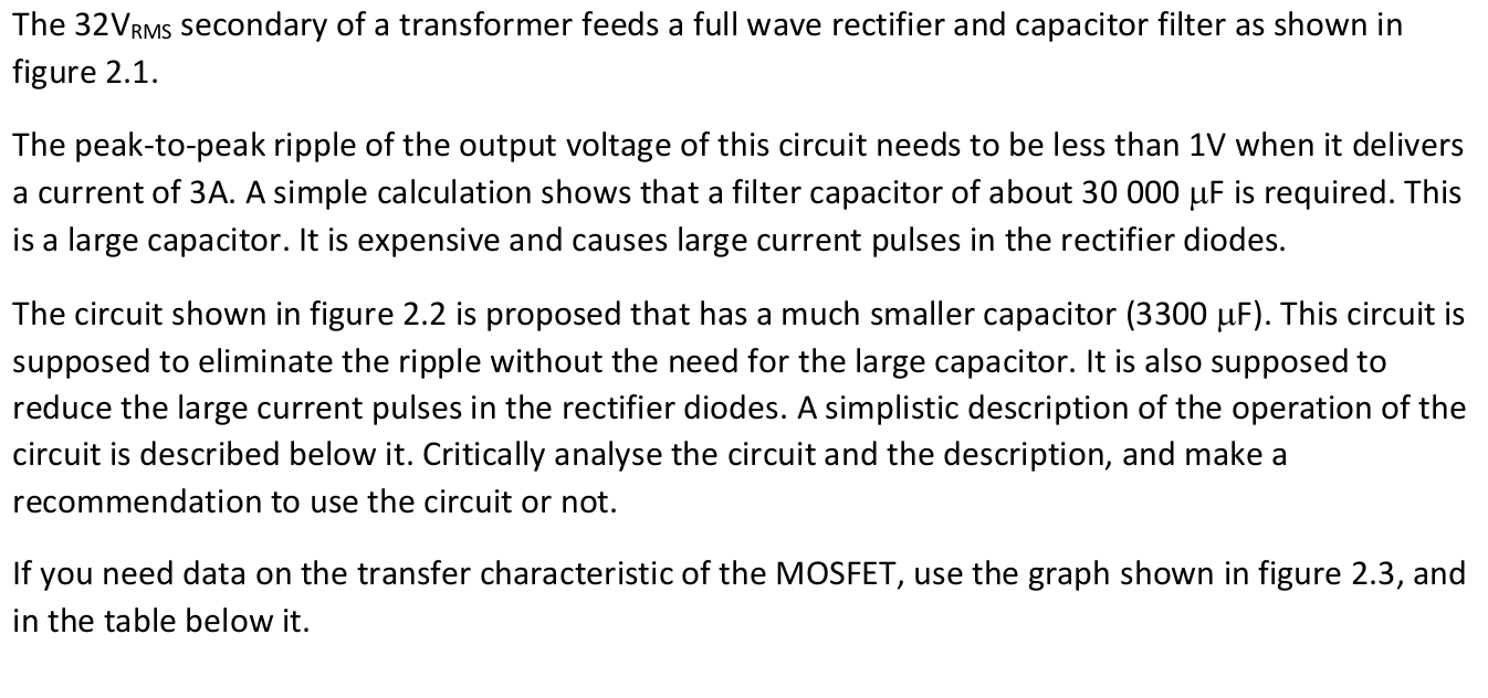
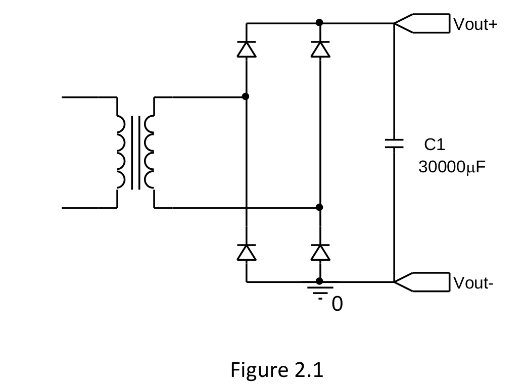
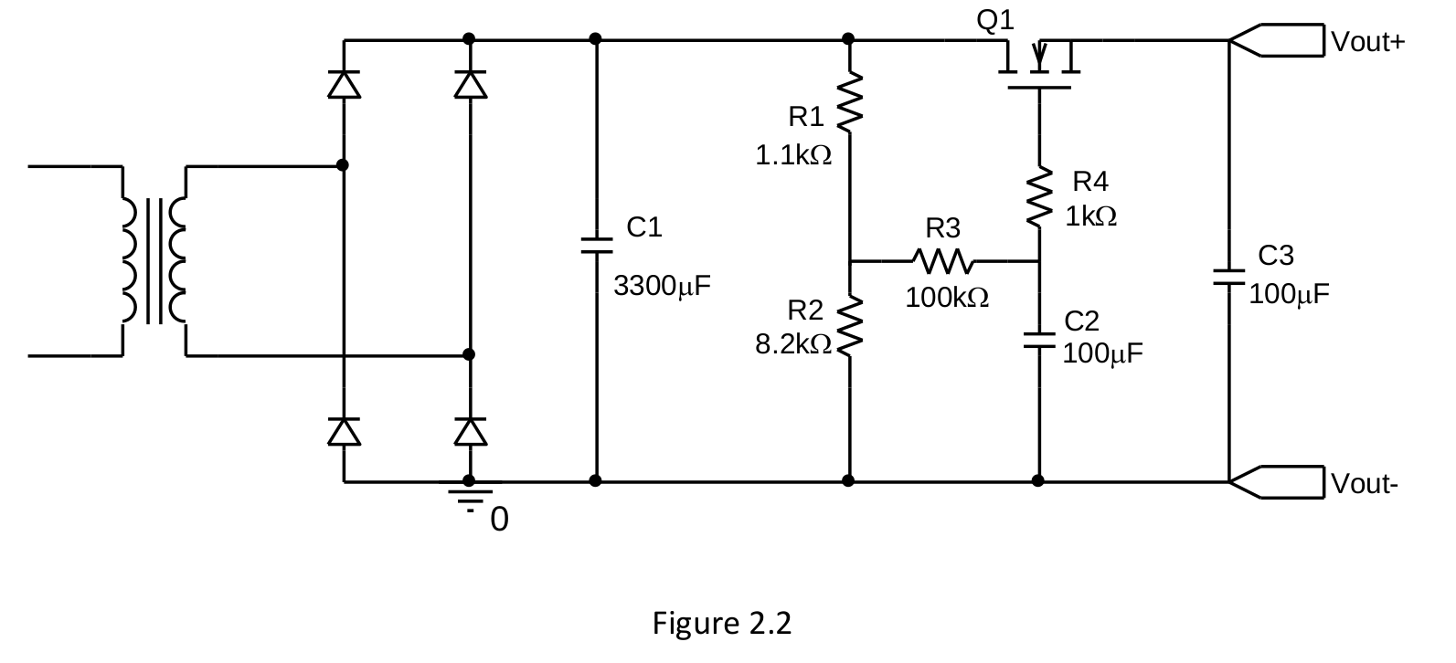
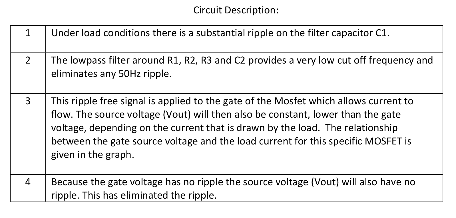
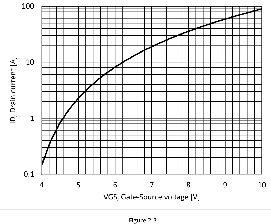
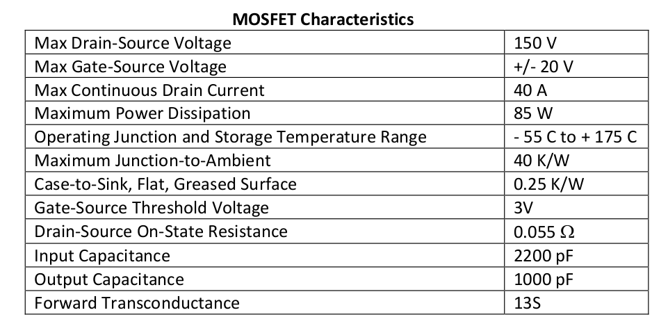
The 32VRMs secondary of a transformer feeds a full wave rectifier and capacitor filter as shown in figure 2.1. The peak-to-peak ripple of the output voltage of this circuit needs to be less than 1V when it delivers a current of 3A. A simple calculation shows that a filter capacitor about 30 000 uF is required. This is a large capacitor. It is expensive and causes large current pulses in the rectifier diodes. The circuit shown in figure 2.2 is proposed that has a much smaller capacitor (3300 uF). This circuit is supposed to eliminate the ripple without the need for the large capacitor. It is also supposed to reduce the large current pulses in the rectifier diodes. A simplistic description of the operation of the circuit is described below it. Critically analyse the circuit and the description, and make a recommendation to use the circuit or not. If you need data on the transfer characteristic of the MOSFET, use the graph shown in figure 2.3, and in the table below it. Vout+ $ C1 30000uF Vout- Figure 2.1 Q1 Vout+ 11 $ R1 1.1k R4 1k C1 R3 HE 3300uF C3 T100 F 100k2 R2 8.2k12 C2 100uF a Vout- Figure 2.2 Circuit Description: 1 Under load conditions there is a substantial ripple on the filter capacitor C1. 2 The lowpass filter around R1, R2, R3 and C2 provides a very low cut off frequency and eliminates any 50Hz ripple. 3 This ripple free signal is applied to the gate of the Mosfet which allows current to flow. The source voltage (Vout) will then also be constant, lower than the gate voltage, depending on the current that is drawn by the load. The relationship between the gate source voltage and the load current for this specific MOSFET is given in the graph. 4 Because the gate voltage has no ripple the source voltage (Vout) will also have no ripple. This has eliminated the ripple. 100 10 ID, Drain current [A] 0.1 5 9 10 6 7 8 VGS, Gate-Source voltage [V] Figure 2.3 MOSFET Characteristics Max Drain-Source Voltage Max Gate-Source Voltage Max Continuous Drain Current Maximum Power Dissipation Operating Junction and Storage Temperature Range Maximum Junction-to-Ambient Case-to-Sink, Flat, Greased Surface Gate-Source Threshold Voltage Drain-Source On-State Resistance Input Capacitance Output Capacitance Forward Transconductance 150 V +/- 20 V 40 A 85 W -55 C to + 175 C 40 K/W 0.25 K/W 3V 0.055 22 2200 pF 1000 pF 13S The 32VRMs secondary of a transformer feeds a full wave rectifier and capacitor filter as shown in figure 2.1. The peak-to-peak ripple of the output voltage of this circuit needs to be less than 1V when it delivers a current of 3A. A simple calculation shows that a filter capacitor about 30 000 uF is required. This is a large capacitor. It is expensive and causes large current pulses in the rectifier diodes. The circuit shown in figure 2.2 is proposed that has a much smaller capacitor (3300 uF). This circuit is supposed to eliminate the ripple without the need for the large capacitor. It is also supposed to reduce the large current pulses in the rectifier diodes. A simplistic description of the operation of the circuit is described below it. Critically analyse the circuit and the description, and make a recommendation to use the circuit or not. If you need data on the transfer characteristic of the MOSFET, use the graph shown in figure 2.3, and in the table below it. Vout+ $ C1 30000uF Vout- Figure 2.1 Q1 Vout+ 11 $ R1 1.1k R4 1k C1 R3 HE 3300uF C3 T100 F 100k2 R2 8.2k12 C2 100uF a Vout- Figure 2.2 Circuit Description: 1 Under load conditions there is a substantial ripple on the filter capacitor C1. 2 The lowpass filter around R1, R2, R3 and C2 provides a very low cut off frequency and eliminates any 50Hz ripple. 3 This ripple free signal is applied to the gate of the Mosfet which allows current to flow. The source voltage (Vout) will then also be constant, lower than the gate voltage, depending on the current that is drawn by the load. The relationship between the gate source voltage and the load current for this specific MOSFET is given in the graph. 4 Because the gate voltage has no ripple the source voltage (Vout) will also have no ripple. This has eliminated the ripple. 100 10 ID, Drain current [A] 0.1 5 9 10 6 7 8 VGS, Gate-Source voltage [V] Figure 2.3 MOSFET Characteristics Max Drain-Source Voltage Max Gate-Source Voltage Max Continuous Drain Current Maximum Power Dissipation Operating Junction and Storage Temperature Range Maximum Junction-to-Ambient Case-to-Sink, Flat, Greased Surface Gate-Source Threshold Voltage Drain-Source On-State Resistance Input Capacitance Output Capacitance Forward Transconductance 150 V +/- 20 V 40 A 85 W -55 C to + 175 C 40 K/W 0.25 K/W 3V 0.055 22 2200 pF 1000 pF 13SStep by Step Solution
There are 3 Steps involved in it
Step: 1

Get Instant Access to Expert-Tailored Solutions
See step-by-step solutions with expert insights and AI powered tools for academic success
Step: 2

Step: 3
Ace Your Homework with AI
Get the answers you need in no time with our AI-driven, step-by-step assistance
Get Started
ERP Digital License Management Audit And Compliance
Authors: Gangesh Thakur, Jay Kalaimani
1st Edition
1799104079, 978-1799104070