Answered step by step
Verified Expert Solution
Question
1 Approved Answer
Derive an equation that defines the worst case low-high propagation delay for a Static CMOS 4-input NOR gate. Use the Resistor-Switch model to illustrate your
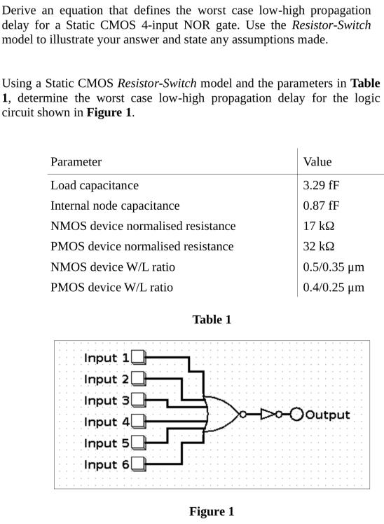
Derive an equation that defines the worst case low-high propagation delay for a Static CMOS 4-input NOR gate. Use the Resistor-Switch model to illustrate your answer and state any assumptions made. Using a Static CMOS Resistor-Switch model and the parameters in Table 1, determine the worst case low-high propagation delay for the logic circuit shown in Figure 1. Value 3.29 fF 0.87 fF Parameter Load capacitance Internal node capacitance NMOS device normalised resistance PMOS device normalised resistance NMOS device W/L ratio PMOS device W/L ratio 17 k92 32 k2 0.5/0.35 um 0.4/0.25 um Table 1 Input 1 Input 2 Input 3 Input 4 Input 5 Input 6! > Doutput Figure 1
Step by Step Solution
There are 3 Steps involved in it
Step: 1
Get Instant Access to Expert-Tailored Solutions
See step-by-step solutions with expert insights and AI powered tools for academic success
Step: 2
Step: 3
Ace Your Homework with AI
Get the answers you need in no time with our AI-driven, step-by-step assistance
Get Started