Answered step by step
Verified Expert Solution
Link Copied!

Question

1 Approved Answer

Design Objective: You will design an 16 x 4 SRAM by extending the SRAM shown in figure 16. The output of this SRAM will be
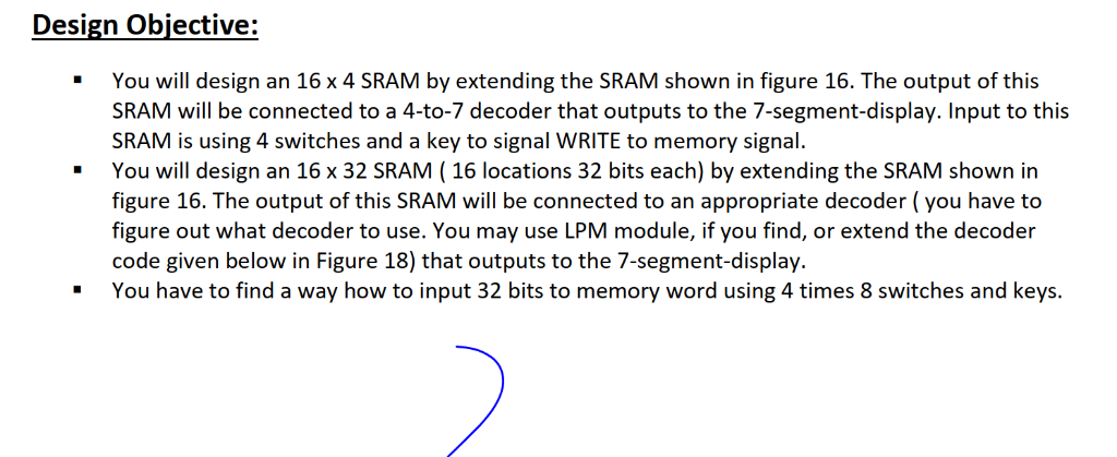
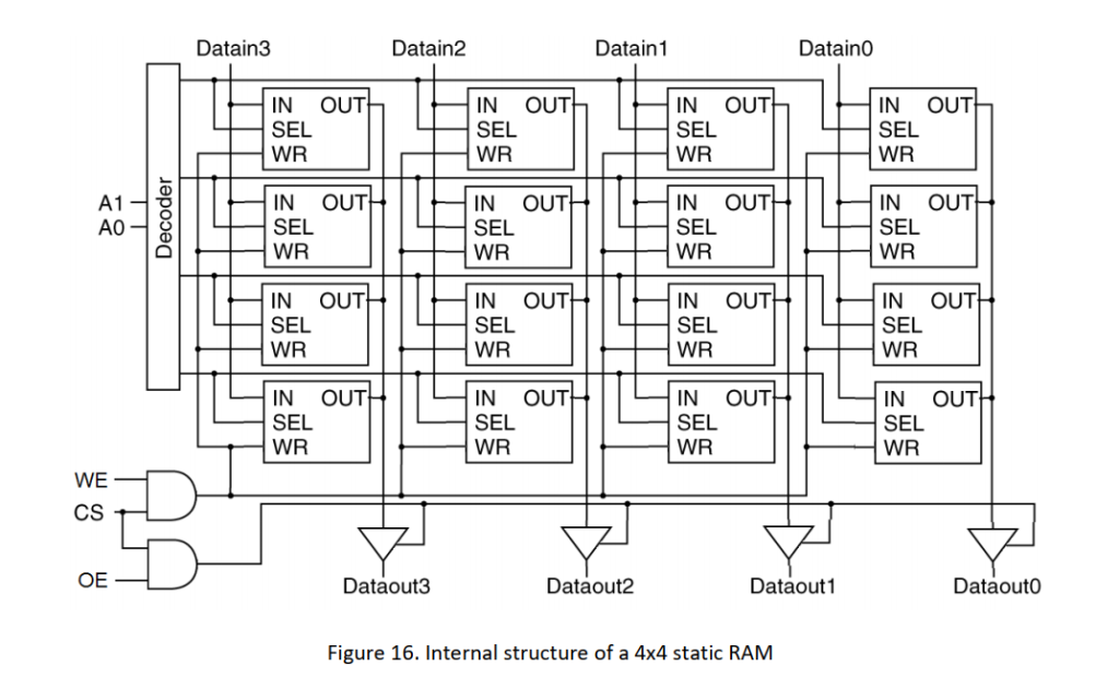
image text in transcribedimage text in transcribed

Design Objective: You will design an 16 x 4 SRAM by extending the SRAM shown in figure 16. The output of this SRAM will be connected to a 4-to-7 decoder that outputs to the 7-segment-display. Input to this SRAM is using 4 switches and a key to signal WRITE to memory signal figure 16. The output of this SRAM will be connected to an appropriate decoder(you have to code given below in Figure 18) that outputs to the 7-segment-display. You will design an 16 x 32 SRAM (16 locations 32 bits each) by extending the SRAM shown in M module, if you find You have to find a way how to input 32 bits to memory word using 4 times 8 switches and keys. Datain3 Datain2 Datain1 DatainO IN OUT SEL WR IN OUT SEL WR IN OUT SEL WR IN OUT SEL WR IN OUT SEL WR IN OUT SEL WR IN OUT SEL WR IN OUT SEL WR IN OUT SEL WR IN OUT SEL WR IN OUT SEL WR IN OUT SEL WR IN OUT SEL WR IN OUT SEL WR IN OUT SEL WR IN OUT SEL WR WE CS OE Dataout3 Dataout2 Dataout1 Dataout0 Figure 16. Internal structure of a 4x4 static RAM Design Objective: You will design an 16 x 4 SRAM by extending the SRAM shown in figure 16. The output of this SRAM will be connected to a 4-to-7 decoder that outputs to the 7-segment-display. Input to this SRAM is using 4 switches and a key to signal WRITE to memory signal figure 16. The output of this SRAM will be connected to an appropriate decoder(you have to code given below in Figure 18) that outputs to the 7-segment-display. You will design an 16 x 32 SRAM (16 locations 32 bits each) by extending the SRAM shown in M module, if you find You have to find a way how to input 32 bits to memory word using 4 times 8 switches and keys. Datain3 Datain2 Datain1 DatainO IN OUT SEL WR IN OUT SEL WR IN OUT SEL WR IN OUT SEL WR IN OUT SEL WR IN OUT SEL WR IN OUT SEL WR IN OUT SEL WR IN OUT SEL WR IN OUT SEL WR IN OUT SEL WR IN OUT SEL WR IN OUT SEL WR IN OUT SEL WR IN OUT SEL WR IN OUT SEL WR WE CS OE Dataout3 Dataout2 Dataout1 Dataout0 Figure 16. Internal structure of a 4x4 static RAM

Step by Step Solution

There are 3 Steps involved in it

Step: 1

blur-text-image

Get Instant Access to Expert-Tailored Solutions

See step-by-step solutions with expert insights and AI powered tools for academic success

Step: 2

blur-text-image

Step: 3

blur-text-image

Ace Your Homework with AI

Get the answers you need in no time with our AI-driven, step-by-step assistance

Get Started

Recommended Textbook for

Logics For Databases And Information Systems

Authors: Jan Chomicki ,Gunter Saake

1st Edition

1461375827, 978-1461375821

More Books

Students also viewed these Databases questions