

Answered step by step
Verified Expert Solution
Question
1 Approved Answer
digital circuit design 2 Given the following ASM Chart: TO 0 S 1 A Input1 B Input2 N Input3 F 0 T2 F - T3
digital circuit design 2 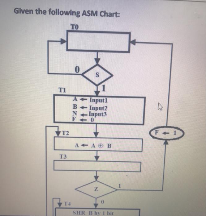
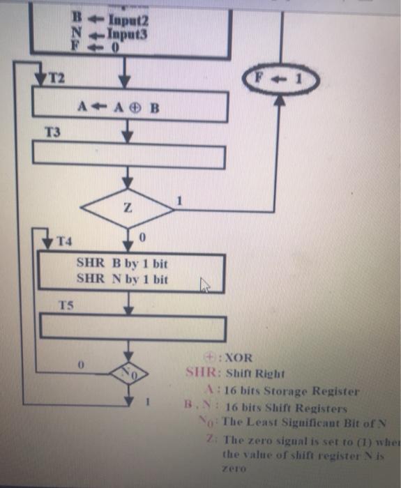

Given the following ASM Chart: TO 0 S 1 A Input1 B Input2 N Input3 F 0 T2 F - T3 1 z 14 0 SHR B by 1 bit B Input2 N -Input3 FO T2 F - T3 Z T4 0 SHR B by 1 bit SHR N by 1 bit TS 0 +: XOR SHIR: Shin Right 1:16 bits Storage Register B.: 16 bits Shift Registers No The Least Significant Bit of N Z: The zero signal is set to (1) wher the value of shin register is 1) Design the data processor (You have to show the data source and the control signals for each component. (10 Points) 2) Design the controller using one flip-flop per state (You have to show the clock and the reset signals) (5 Points) Step by Step Solution
There are 3 Steps involved in it
Step: 1

Get Instant Access to Expert-Tailored Solutions
See step-by-step solutions with expert insights and AI powered tools for academic success
Step: 2

Step: 3
Ace Your Homework with AI
Get the answers you need in no time with our AI-driven, step-by-step assistance
Get Started
Database Modeling And Design
Authors: Toby J. Teorey, Sam S. Lightstone, Tom Nadeau, H.V. Jagadish
5th Edition
0123820200, 978-0123820204