

Question: Do Problem 2.Problem 2. Problem 2.Problem 2 thx 2. Suppose the main memory in Problem 1 is divided into four memory banks. The access time
Do Problem 2.Problem 2.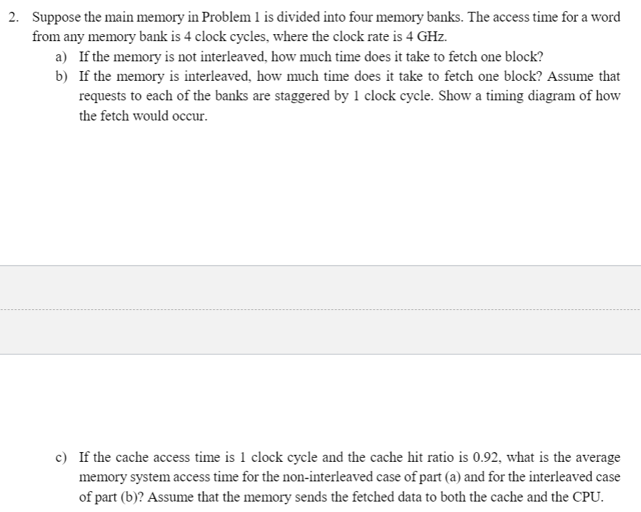 Problem 2.Problem 2 thx
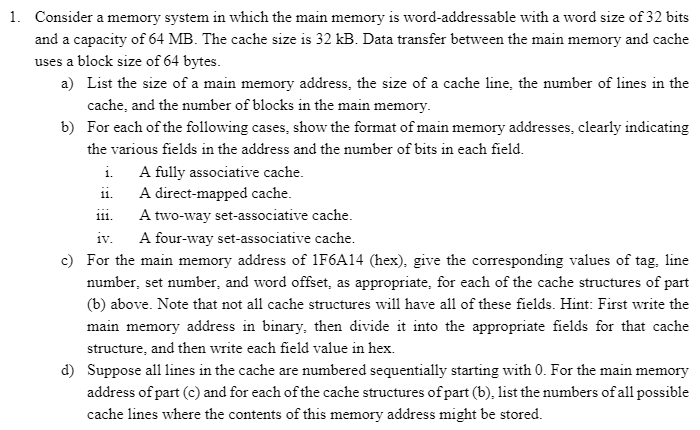
2. Suppose the main memory in Problem 1 is divided into four memory banks. The access time for a word from any memory bank is 4 clock cycles, where the clock rate is 4 GHz. a) If the memory is not interleaved, how much time does it take to fetch one block? b) If the memory is interleaved, how much time does it take to fetch one block? Assume that requests to each of the banks are staggered by 1 clock cycle. Show a timing diagram of how the fetch would occur. c) If the cache access time is 1 clock cycle and the cache hit ratio is 0.92, what is the average memory system access time for the non-interleaved case of part (a) and for the interleaved case of part (b)? Assume that the memory sends the fetched data to both the cache and the CPU. 1. Consider a memory system in which the main memory is word-addressable with a word size of 32 bits and a capacity of 64 MB. The cache size is 32 kB. Data transfer between the main memory and cache uses a block size of 64 bytes. a) List the size of a main memory address, the size of a cache line, the number of lines in the cache and the number of blocks in the main memory. b) For each of the following cases, show the format of main memory addresses, clearly indicating the various fields in the address and the number of bits in each field. i. A fully associative cache. ii. A direct-mapped cache. 111. A two-way set-associative cache. iv. A four-way set-associative cache. c) For the main memory address of 1F6A14 (hex), give the corresponding values of tag, line number, set number, and word offset, as appropriate, for each of the cache structures of part (b) above. Note that not all cache structures will have all of these fields. Hint: First write the main memory address in binary, then divide it into the appropriate fields for that cache structure, and then write each field value in hex. d) Suppose all lines in the cache are numbered sequentially starting with 0. For the main memory address of part (c) and for each of the cache structures of part (b), list the numbers of all possible cache lines where the contents of this memory address might be stored. 2. Suppose the main memory in Problem 1 is divided into four memory banks. The access time for a word from any memory bank is 4 clock cycles, where the clock rate is 4 GHz. a) If the memory is not interleaved, how much time does it take to fetch one block? b) If the memory is interleaved, how much time does it take to fetch one block? Assume that requests to each of the banks are staggered by 1 clock cycle. Show a timing diagram of how the fetch would occur. c) If the cache access time is 1 clock cycle and the cache hit ratio is 0.92, what is the average memory system access time for the non-interleaved case of part (a) and for the interleaved case of part (b)? Assume that the memory sends the fetched data to both the cache and the CPU. 1. Consider a memory system in which the main memory is word-addressable with a word size of 32 bits and a capacity of 64 MB. The cache size is 32 kB. Data transfer between the main memory and cache uses a block size of 64 bytes. a) List the size of a main memory address, the size of a cache line, the number of lines in the cache and the number of blocks in the main memory. b) For each of the following cases, show the format of main memory addresses, clearly indicating the various fields in the address and the number of bits in each field. i. A fully associative cache. ii. A direct-mapped cache. 111. A two-way set-associative cache. iv. A four-way set-associative cache. c) For the main memory address of 1F6A14 (hex), give the corresponding values of tag, line number, set number, and word offset, as appropriate, for each of the cache structures of part (b) above. Note that not all cache structures will have all of these fields. Hint: First write the main memory address in binary, then divide it into the appropriate fields for that cache structure, and then write each field value in hex. d) Suppose all lines in the cache are numbered sequentially starting with 0. For the main memory address of part (c) and for each of the cache structures of part (b), list the numbers of all possible cache lines where the contents of this memory address might be stored
Step by Step Solution
There are 3 Steps involved in it

Get step-by-step solutions from verified subject matter experts