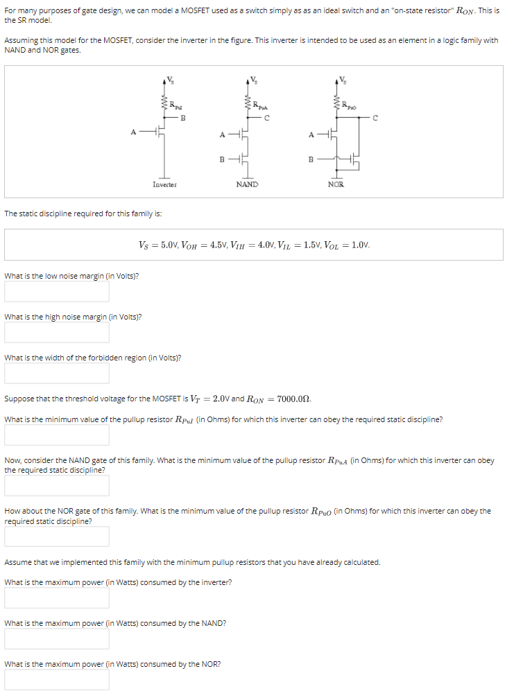
For many purposes of gate design, we can model a MOSFET used as a switch simply as as an ideal switch and an on-state

For many purposes of gate design, we can model a MOSFET used as a switch simply as as an ideal switch and an "on-state resistor" RON- This is the SR model. Assuming this model for the MOSFET, consider the inverter in the figure. This inverter is intended to be used as an element in a logic family with NAND and NOR gates. A HE AHE BHE Invecter NAND NOR The static discipline required for this family is: Vs = 5.0V, Von = 4.5V, VIH = 4.0V, VIL = 1.5V, Vor = 1.0V. What is the low noise margin (in Volts)? What is the high noise margin (in Volts)? What is the width of the forbidden region (in Volts)? Suppose that the threshold voltage for the MOSFET is Vr = 2.0V and RoN = 7000.0n. What is the minimum value of the pullup resistor RPu (in Ohms) for which this inverter can obey the required static discipline? Now, consider the NAND gate of this family. What is the minimum value of the pullup resistor RPuA (in Ohms) for which this inverter can obey the required static discipline? How about the NOR gate of this family. What is the minimum value of the pullup resistor RPuo (in Ohms) for which this inverter can obey the required static discipline? Assume that we implemented this family with the minimum pullup resistors that you have already calculated. What is the maximum power (in Watts) consumed by the inverter? What is the maximum power (in Watts) consumed by the NAND? What is the maximum power (in Watts) consumed by the NOR?
Step by Step Solution
3.33 Rating (144 Votes )
There are 3 Steps involved in it
Step: 1
Vs Vs A Inveatea NOR fig ces NAND fig cb Given Vsso...
See step-by-step solutions with expert insights and AI powered tools for academic success
Step: 2

Step: 3

Ace Your Homework with AI
Get the answers you need in no time with our AI-driven, step-by-step assistance
Get Started


