

Question: For this task, you will design a small instruction decoder and executor, which is at the heart of a processor. This should be done either
For this task, you will design a small instruction decoder and executor, which is at the heart of a processor. This should be done either on paper or in a file named executor.jpg. This component will use the components you designed in tasks 1 and 2, in an abstract manner. The processor instuctions you will be working with are described thusly.
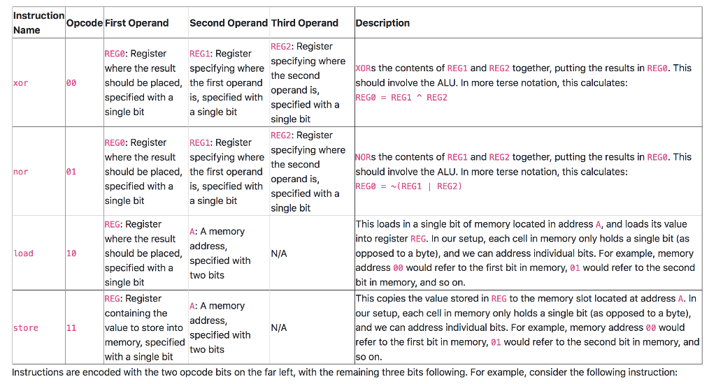
Instructions are uniformly encoded with 5 bits, and there are four instructions in total. The first two bits of the instructions encode the opcode, which is used to differentiate between instruction types. The next three bits encode which registers the instruction operates on, or a memory address, depending on the particular instruction. Registers are specified using a single bit, and memory addresses are specified with two bits. A table of all the possible instructions is below.
Restrictions:
CAN ONLY USE THE FOLLOWING !!
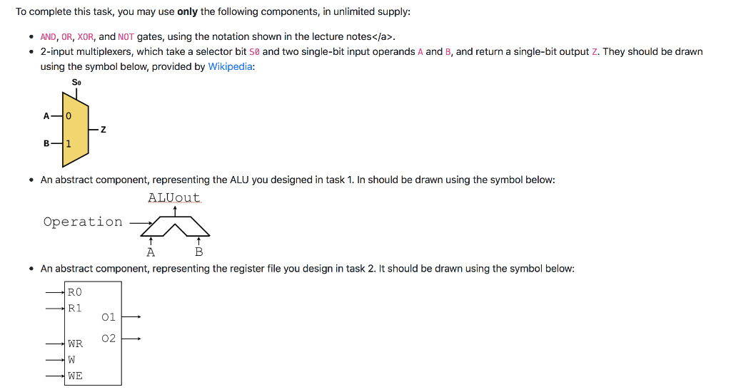
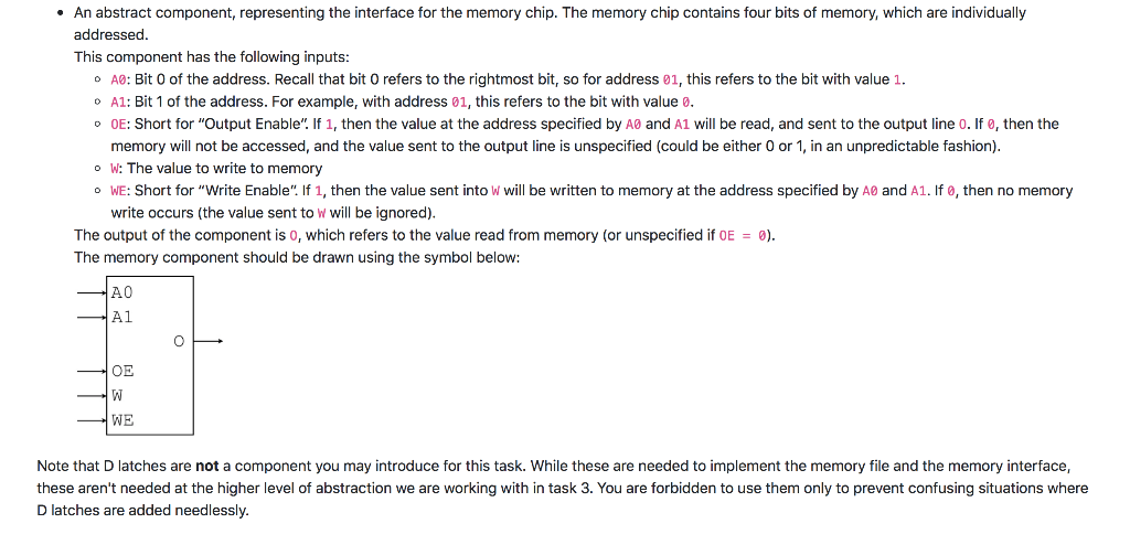
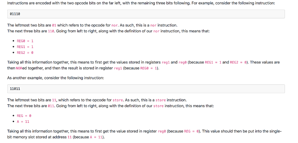
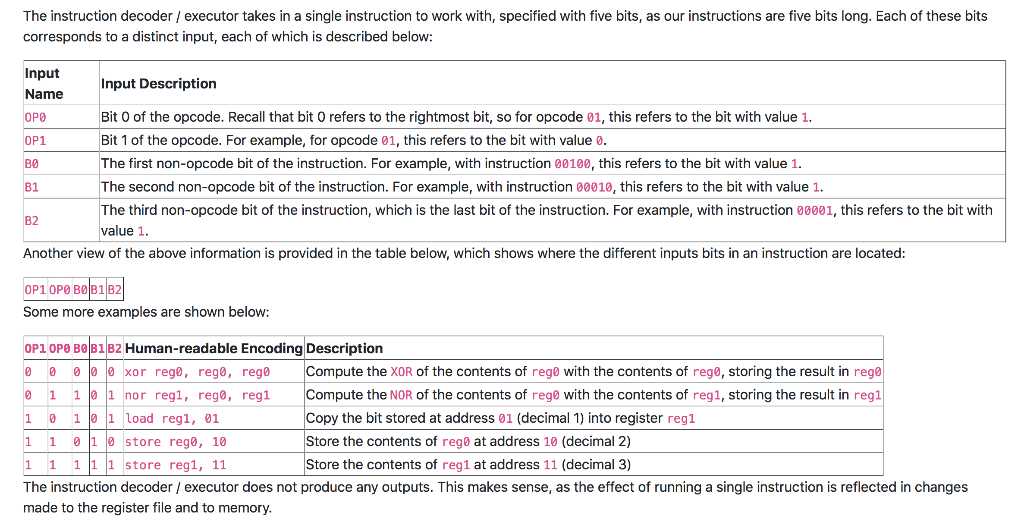
Instructions are encoded with the two opcode bits on the far left, with the remaining three bits following. For example, consider the following instruction: 01110 The leftmost two bits are 01 which refers to the opcode for nor. As such, this is a nor instruction. The next three bits are 110. Going from left to right, along with the definition of our nor instruction, this means that REGO1 REG20 Taking all this information together, this means to first get the values stored in registers regl and rego (because REG1-1 and REG2 = 0). These values are then NoRed together, and then the result is stored in register reg1 (because REGe1 As another example, consider the following instruction: 11011 The leftmost two bits are 11, which refers to the opcode for store. As such, this is a store instruction. The next three bits are 011. Going from left to right, along with the definition of our store instruction, this means that: REG- A 11 Taking all this information together, this means to first get the value stored in register reg0 (because REG 0). This value should then be put into the single bit memory slot stored at address 11 (because A 11) The instruction decoder / executor takes in a single instruction to work with, specified with five bits, as our instructions are five bits long. Each of these bits corresponds to a distinct input, each of which is described below: Input Name OP0 OP1 B1 Input Description Bit O of the opcode. Recall that bit O refers to the rightmost bit, so for opcode 01, this refers to the bit with value 1. Bit 1 of the opcode. For example, for opcode 01, this refers to the bit with value 0. The first non-opcode bit of the instruction. For example, with instruction 00100, this refers to the bit with value 1 The second non-opcode bit of the instruction. For example, with instruction 00010, this refers to the bit with value1 The third non-opcode bit of the instruction, which is the last bit of the instruction. For example, with instruction 00001, this refers to the bit with value 1 B2 Another view of the above information is provided in the table below, which shows where the different inputs bits in an instruction are located P1P B0B1 82 Some more examples are shown below: OP1OPO B0 B1B2 Human-readable Encoding Description 0 000 xor rege, reg0, reg 0 1 11 nor regl, reg0, reg1 1 0 11 load regl, 01 1 1 0 10 store rego, 10 Compute the XOR of the contents of reg with the contents of rege, storing the result in reg Compute the NOR of the contents of reg with the contents of reg1, storing the result in reg1 Copy the bit stored at address 01 (decimal 1) into register regl Store the contents of reg at address 10 (decimal 2) Store the contents of reg1 at address 11 (decimal 3) The instruction decoder executor does not produce any outputs. This makes sense, as the effect of running a single instruction is reflected in changes made to the register file and to memory To complete this task, you may use only the following components, in unlimited supply: AND, OR, XOR, and NOT gates, using the notation shown in the lecture notes 2-input multiplexers, which take a selector bit S0 and two single-bit input operands A and B, and return a single-bit output Z. They should be drawn using the symbol below, provided by Wikipedia: So A O B-1 An abstract component, representing the ALU you designed in task 1. In should be drawn using the symbol below: ALUout Operation An abstract component, representing the register file you design in task 2. It should be drawn using the symbol below: RO R1 01 WR 02 WE .An abstract component, representing the interface for the memory chip. The memory chip contains four bits of memory, which are individually addressed. This component has the following inputs: o A0: Bit 0 of the address. Recall that bit 0 refers to the rightmost bit, so for address 01, this refers to the bit with value 1 o A1: Bit 1 of the address. For example, with address 01, this refers to the bit with value0 o OE: Short for "Output Enable". If 1, then the value at the address specified by A0 and A1 will be read, and sent to the output line 0. If e, then the memory will not be accessed, and the value sent to the output line is unspecified (could be either 0 or 1, in an unpredictable fashion) o W: The value to write to memory WE: Short for "write Enable". If 1, then the value sent into w will be written to memory at the address specified by A0 and A1. If 0, then no memory write occurs (the value sent to W will be ignored) The output of the component is o, which refers to the value read from memory (or unspecified it The memory component should be drawn using the symbol below: A0 A1 WE Note that D latches are not a component you may introduce for this task. While these are needed to implement the memory file and the memory interface, these aren't needed at the higher level of abstraction we are working with in task 3. You are forbidden to use them only to prevent confusing situations where D latches are added needlessly Instructions are encoded with the two opcode bits on the far left, with the remaining three bits following. For example, consider the following instruction: 01110 The leftmost two bits are 01 which refers to the opcode for nor. As such, this is a nor instruction. The next three bits are 110. Going from left to right, along with the definition of our nor instruction, this means that REGO1 REG20 Taking all this information together, this means to first get the values stored in registers regl and rego (because REG1-1 and REG2 = 0). These values are then NoRed together, and then the result is stored in register reg1 (because REGe1 As another example, consider the following instruction: 11011 The leftmost two bits are 11, which refers to the opcode for store. As such, this is a store instruction. The next three bits are 011. Going from left to right, along with the definition of our store instruction, this means that: REG- A 11 Taking all this information together, this means to first get the value stored in register reg0 (because REG 0). This value should then be put into the single bit memory slot stored at address 11 (because A 11) The instruction decoder / executor takes in a single instruction to work with, specified with five bits, as our instructions are five bits long. Each of these bits corresponds to a distinct input, each of which is described below: Input Name OP0 OP1 B1 Input Description Bit O of the opcode. Recall that bit O refers to the rightmost bit, so for opcode 01, this refers to the bit with value 1. Bit 1 of the opcode. For example, for opcode 01, this refers to the bit with value 0. The first non-opcode bit of the instruction. For example, with instruction 00100, this refers to the bit with value 1 The second non-opcode bit of the instruction. For example, with instruction 00010, this refers to the bit with value1 The third non-opcode bit of the instruction, which is the last bit of the instruction. For example, with instruction 00001, this refers to the bit with value 1 B2 Another view of the above information is provided in the table below, which shows where the different inputs bits in an instruction are located P1P B0B1 82 Some more examples are shown below: OP1OPO B0 B1B2 Human-readable Encoding Description 0 000 xor rege, reg0, reg 0 1 11 nor regl, reg0, reg1 1 0 11 load regl, 01 1 1 0 10 store rego, 10 Compute the XOR of the contents of reg with the contents of rege, storing the result in reg Compute the NOR of the contents of reg with the contents of reg1, storing the result in reg1 Copy the bit stored at address 01 (decimal 1) into register regl Store the contents of reg at address 10 (decimal 2) Store the contents of reg1 at address 11 (decimal 3) The instruction decoder executor does not produce any outputs. This makes sense, as the effect of running a single instruction is reflected in changes made to the register file and to memory To complete this task, you may use only the following components, in unlimited supply: AND, OR, XOR, and NOT gates, using the notation shown in the lecture notes 2-input multiplexers, which take a selector bit S0 and two single-bit input operands A and B, and return a single-bit output Z. They should be drawn using the symbol below, provided by Wikipedia: So A O B-1 An abstract component, representing the ALU you designed in task 1. In should be drawn using the symbol below: ALUout Operation An abstract component, representing the register file you design in task 2. It should be drawn using the symbol below: RO R1 01 WR 02 WE .An abstract component, representing the interface for the memory chip. The memory chip contains four bits of memory, which are individually addressed. This component has the following inputs: o A0: Bit 0 of the address. Recall that bit 0 refers to the rightmost bit, so for address 01, this refers to the bit with value 1 o A1: Bit 1 of the address. For example, with address 01, this refers to the bit with value0 o OE: Short for "Output Enable". If 1, then the value at the address specified by A0 and A1 will be read, and sent to the output line 0. If e, then the memory will not be accessed, and the value sent to the output line is unspecified (could be either 0 or 1, in an unpredictable fashion) o W: The value to write to memory WE: Short for "write Enable". If 1, then the value sent into w will be written to memory at the address specified by A0 and A1. If 0, then no memory write occurs (the value sent to W will be ignored) The output of the component is o, which refers to the value read from memory (or unspecified it The memory component should be drawn using the symbol below: A0 A1 WE Note that D latches are not a component you may introduce for this task. While these are needed to implement the memory file and the memory interface, these aren't needed at the higher level of abstraction we are working with in task 3. You are forbidden to use them only to prevent confusing situations where D latches are added needlessly
Step by Step Solution
There are 3 Steps involved in it

Get step-by-step solutions from verified subject matter experts