

Answered step by step
Verified Expert Solution
Question
1 Approved Answer
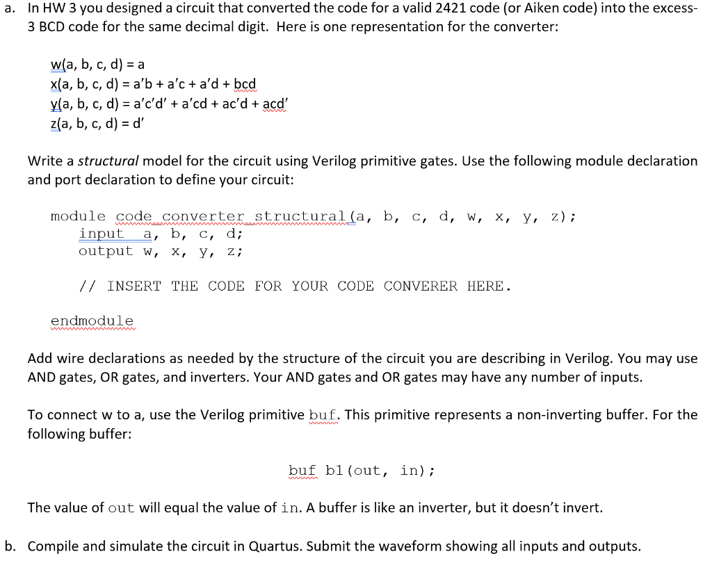
In HW 3 you designed a circuit that converted the code for a valid 2421 code (or Aiken code) into the excess- 3 BCD code
Step by Step Solution
There are 3 Steps involved in it
Step: 1

Get Instant Access to Expert-Tailored Solutions
See step-by-step solutions with expert insights and AI powered tools for academic success
Step: 2

Step: 3
Ace Your Homework with AI
Get the answers you need in no time with our AI-driven, step-by-step assistance
Get Started
Relational Database And Transact SQL
Authors: Lucy Scott
1st Edition
1974679985, 978-1974679980