Answered step by step
Verified Expert Solution
Question
1 Approved Answer
In this lab, we will design a current mirror and an active-loaded differential amplifier, and analyze their characteristics using HSPICE simulation. The device models are
In this lab, we will design a current mirror and an active-loaded differential amplifier, and analyze their characteristics using HSPICE simulation. The device models are from the textbook device library sedra_mod_lib given. You need to analyze the circuits analytically first, and then start the simulation.


I just need the code in hspice, it should be commented just a code please
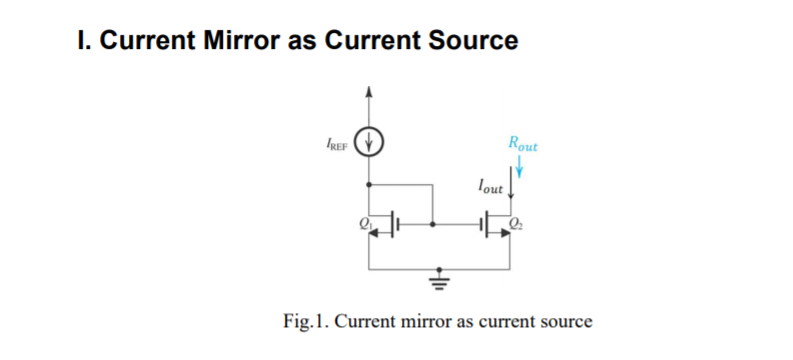
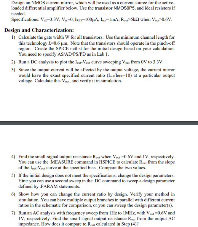
I. Current Mirror as Current Source IREF Rout lout Fig.1. Current mirror as current source Design an NMOS current mirror, which will be used as a current source for the active- loaded differential amplifier below. Use the transistor NMOSOP5, and ideal resistors if needed. Specifications: Vdd-3.3V, V 0, IREF 100uA, Iou-lmA, Rou 5k2 when Vou 0.6V. Design and Characterization: 1) Calculate the gate width W for all transistors. Use the minimum channel length for this technology L-0.6 um. Note that the transistors should operate in the pinch-off region. Create the SPICE netlist for the initial design based on your calculation. You need to specify AS/AD/PS/PD as in Lab 2) Run a DC analysis to plot the lour-Vout curve sweeping Vout from 0V to 3.3V. 3) Since the output current will be affected by the output voltage, the current mirror would have the exact specified current ratio (lou/IREF 10) at a particular output voltage. Calculate this Vout, and verify it in simulation. 4) Find the small-signal output resistance Rout when Vout-0.6V and 1V, respectively. You can use the MEASURE command in HSPICE to calculate Rout from the slope of the lout-Vout curve at the specified bias. Compare the two values If the initial design does not meet the specifications, change the design parameters. Hint: you can use a second sweep in the.DC command to sweep a design parameter defined by PARAM statements. orVou cuet tecfied bias. Compare the two values. 5) 6) Show how you can change the current ratio by design. Verify your method in simulation. You can have multiple output branches in parallel with different current ratios in the schematic for comparison, or you can sweep the design parameter(s). 7) Run an AC analysis with frequency sweep from 1Hz to IMHz, with Vout -0.6V and IV, respectively. Find the small-signal output resistance Rout from the output AC impedance. How does it compare to Rout calculated in Step (4)? I. Current Mirror as Current Source IREF Rout lout Fig.1. Current mirror as current source Design an NMOS current mirror, which will be used as a current source for the active- loaded differential amplifier below. Use the transistor NMOSOP5, and ideal resistors if needed. Specifications: Vdd-3.3V, V 0, IREF 100uA, Iou-lmA, Rou 5k2 when Vou 0.6V. Design and Characterization: 1) Calculate the gate width W for all transistors. Use the minimum channel length for this technology L-0.6 um. Note that the transistors should operate in the pinch-off region. Create the SPICE netlist for the initial design based on your calculation. You need to specify AS/AD/PS/PD as in Lab 2) Run a DC analysis to plot the lour-Vout curve sweeping Vout from 0V to 3.3V. 3) Since the output current will be affected by the output voltage, the current mirror would have the exact specified current ratio (lou/IREF 10) at a particular output voltage. Calculate this Vout, and verify it in simulation. 4) Find the small-signal output resistance Rout when Vout-0.6V and 1V, respectively. You can use the MEASURE command in HSPICE to calculate Rout from the slope of the lout-Vout curve at the specified bias. Compare the two values If the initial design does not meet the specifications, change the design parameters. Hint: you can use a second sweep in the.DC command to sweep a design parameter defined by PARAM statements. orVou cuet tecfied bias. Compare the two values. 5) 6) Show how you can change the current ratio by design. Verify your method in simulation. You can have multiple output branches in parallel with different current ratios in the schematic for comparison, or you can sweep the design parameter(s). 7) Run an AC analysis with frequency sweep from 1Hz to IMHz, with Vout -0.6V and IV, respectively. Find the small-signal output resistance Rout from the output AC impedance. How does it compare to Rout calculated in Step (4)
Step by Step Solution
There are 3 Steps involved in it
Step: 1

Get Instant Access to Expert-Tailored Solutions
See step-by-step solutions with expert insights and AI powered tools for academic success
Step: 2

Step: 3

Ace Your Homework with AI
Get the answers you need in no time with our AI-driven, step-by-step assistance
Get Started


