Answered step by step
Verified Expert Solution
Question
1 Approved Answer
need help Answer any 3 questions. Each question is worth 10 points. Total marks: 3 x 10 = 30. 1. Consider an nMOS transistor in
need help 
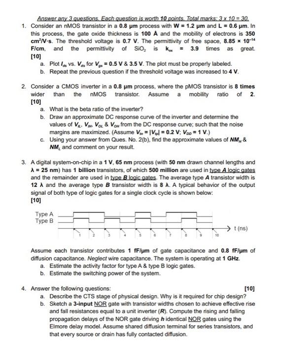
Answer any 3 questions. Each question is worth 10 points. Total marks: 3 x 10 = 30. 1. Consider an nMOS transistor in a 0.8 um process with W = 1.2 um and L = 0.6 um. In this process, the gate oxide thickness is 100 A and the mobility of electrons is 350 cmN-s. The threshold voltage is 0.7 V. The permittivity of free space, 8.85 * 10-14 Ficm, and the permittivity of sio, is k = 3.9 times as great [10] a Ploti, vs. V. for V: = 0.5 V & 3.5V. The plot must be properly labeled. b. Repeat the previous question if the threshold voltage was increased to 4 V. 2. Consider a CMOS inverter in a 0.8 um process, where the PMOS transistor is 8 times wider than the nMOS transistor. Assume a mobility ratio of 2. [10] a. What is the beta ratio of the inverter? b. Draw an approximate DC response curve of the inverter and determine the values of VV VOL & Vow from the DC response curve; such that the noise margins are maximized. (Assume VIVI = 0.2 V; V. = 1 V.) c. Using your answer from Ques. No. 2(b).find the approximate values of NM, & NM, and comment on your result. 3. A digital system-on-chip in a 1 V, 65 nm process (with 50 nm drawn channel lengths and 1 = 25 nm) has 1 billion transistors, of which 500 million are used in type A logic gates and the remainder are used in type B logic gates. The average type A transistor width is 12 and the average type B transistor width is 8 . A typical behavior of the output signal of both type of logic gates for a single clock cycle is shown below: [10] Type A Type B t(ns) Assume each transistor contributes 1 fflum of gate capacitance and 0.8 ff/um of diffusion capacitance. Neglect wire capacitance. The system is operating at 1 GHz. a. Estimate the activity factor for type A & type B logic gates. b. Estimate the switching power of the system. 4. Answer the following questions: [10] a. Describe the CTS stage of physical design. Why is it required for chip design? b. Sketch a 3-input NOR gate with transistor widths chosen to achieve effective rise and fall resistances equal to a unit inverter (R). Compute the rising and falling propagation delays of the NOR gate driving h identical NOR gates using the Elmore delay model. Assume shared diffusion terminal for series transistors, and that every source or drain has fully contacted diffusion 
Step by Step Solution
There are 3 Steps involved in it
Step: 1

Get Instant Access to Expert-Tailored Solutions
See step-by-step solutions with expert insights and AI powered tools for academic success
Step: 2

Step: 3

Ace Your Homework with AI
Get the answers you need in no time with our AI-driven, step-by-step assistance
Get Started


