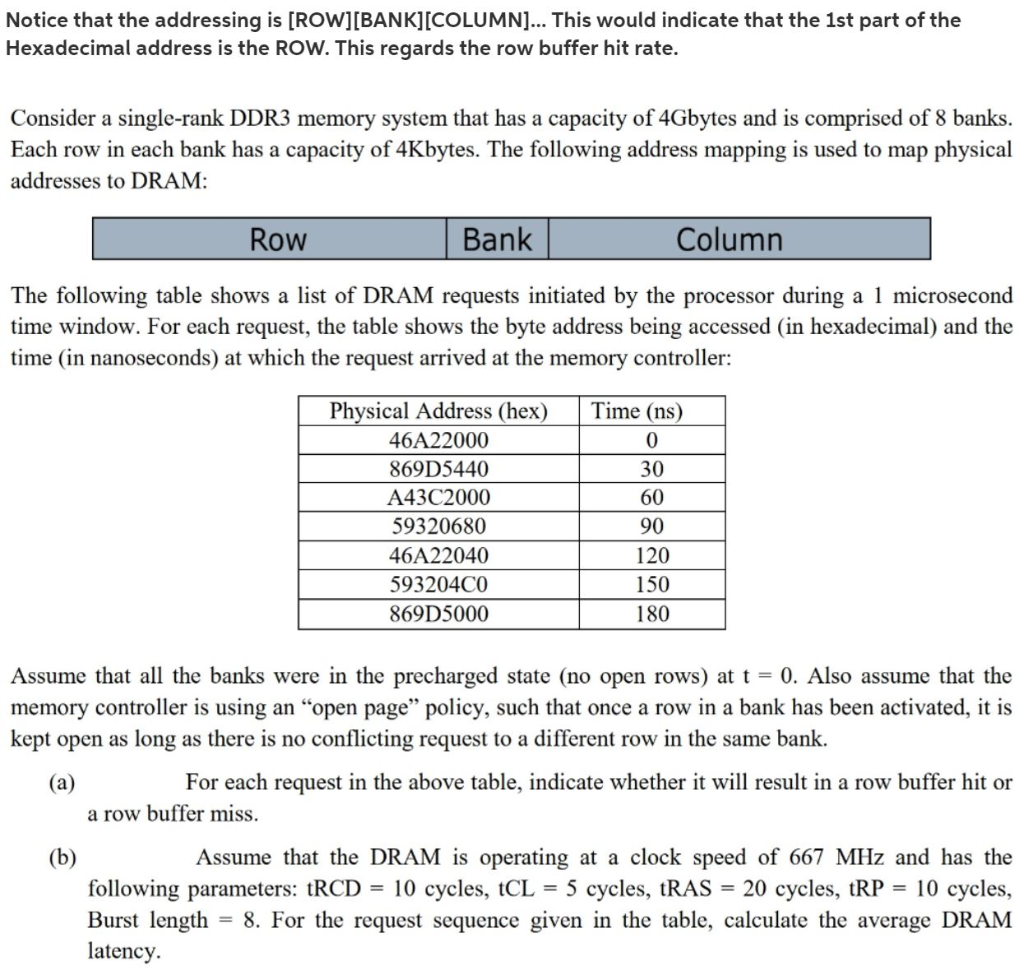
Notice that the addressing is [ROW][BANK][COLUMN]... This would indicate that the 1st part of the Hexadecimal address is the ROW. This regards the row buffer hit rate. Consider a single-rank DDR3 memory system that has a capacity of 4Gbytes and is comprised of 8 banks. Each row in each bank has a capacity of 4Kbytes. The following address mapping is used to map physical addresses to DRAM: Row | Bank Column The following table shows a list of DRAM requests initiated by the processor during a 1 microsecond time window. For each request, the table shows the byte address being accessed (in hexadecimal) and the time (in nanoseconds) at which the request arrived at the memory controller: Time (ns) 0 Physical Address (hex) 46A22000 869D5440 A43C2000 59320680 46A22040 593204CO 869D5000 30 60 90 120 150 180 Assume that all the banks were in the precharged state (no open rows) at t = 0. Also assume that the memory controller is using an open page policy, such that once a row in a bank has been activated, it is kept open as long as there is no conflicting request to a different row in the same bank. (a) For each request in the above table, indicate whether it will result in a row buffer hit or a row buffer miss. Assume that the DRAM is operating at a clock speed of 667 MHz and has the following parameters: tRCD = 10 cycles, tCL = 5 cycles, tRAS = 20 cycles, tRP = 10 cycles, Burst length = 8. For the request sequence given in the table, calculate the average DRAM latency. Notice that the addressing is [ROW][BANK][COLUMN]... This would indicate that the 1st part of the Hexadecimal address is the ROW. This regards the row buffer hit rate. Consider a single-rank DDR3 memory system that has a capacity of 4Gbytes and is comprised of 8 banks. Each row in each bank has a capacity of 4Kbytes. The following address mapping is used to map physical addresses to DRAM: Row | Bank Column The following table shows a list of DRAM requests initiated by the processor during a 1 microsecond time window. For each request, the table shows the byte address being accessed (in hexadecimal) and the time (in nanoseconds) at which the request arrived at the memory controller: Time (ns) 0 Physical Address (hex) 46A22000 869D5440 A43C2000 59320680 46A22040 593204CO 869D5000 30 60 90 120 150 180 Assume that all the banks were in the precharged state (no open rows) at t = 0. Also assume that the memory controller is using an open page policy, such that once a row in a bank has been activated, it is kept open as long as there is no conflicting request to a different row in the same bank. (a) For each request in the above table, indicate whether it will result in a row buffer hit or a row buffer miss. Assume that the DRAM is operating at a clock speed of 667 MHz and has the following parameters: tRCD = 10 cycles, tCL = 5 cycles, tRAS = 20 cycles, tRP = 10 cycles, Burst length = 8. For the request sequence given in the table, calculate the average DRAM latency


