

Question
Objectives Analysis of synchronous finite state machines (FSM) implemented with D- and JK-flip-flops. Description of FSM with state tables and state diagrams, waveform simulation, understanding
Objectives
Analysis of synchronous finite state machines (FSM) implemented with D- and JK-flip-flops. Description of FSM with state tables and state diagrams, waveform simulation, understanding the origin of glitches at the outputs and elimination of the glitches. Calculation of the maximum clock frequency for a reliable system operation.
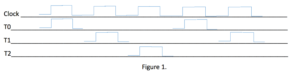
Design descriptions For analysis two variants of the timing signal generators are proposed. Both generators produce the same 3-phase non-overlapping timing signals repeating clock pulses. The output waveforms T0, T1, T2 are shown in Figure 1 for reference. The clock is a square-wave with a 50 % duty cycle, the clock frequency can vary.
Two variants of the system have to be analyzed: variants A and B implemented with D and JK-flip-flops, respectively. The circuit schematics for variants A and B are shown in Figures 2 and 3, respectively. It will be shown that the propagation delay in a flip-flop can result in unwanted glitches at the outputs and how the design can be modified to avoid the glitches.
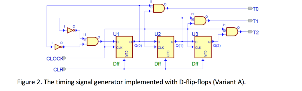
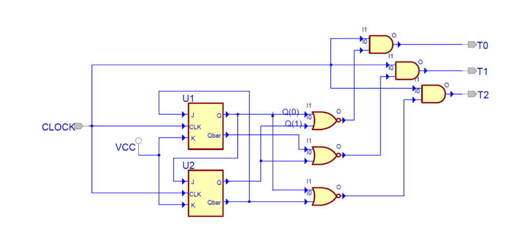
Variant A in Figure 2 was implemented with D-flip-flops using 1-hot state assignment plus 000 (4 used states out of 8 states: 000, 001, 010, 100). The 1-hot assignment offers simplicity of output forming logic: the flip-flop outputs are used for forming the timing signals with AND2 gates. In Variant B (Figure 3) the binary state encoding allowed to use fewer flip-flops (2 instead of 3) at the expense of a state decoder. The latter was implemented with NOR2 gates. For a given task, input excitation equations for JK flip-flops are simpler compared to those for D-flip-flops because of dont cares (): for any transitions QQ*inputs are as follows: J =Q*, K= for Q = 0 and J=, K=Q* for Q = 1. In Variant B JK-flip-flops required no logic gates for input excitation while in Variant A excitation of one D-flip-flop required logic gates.
In both variants (Figures 2 and 3) change of flip-flop states occurs at the rising edges of the clock. Racing of the flip-flop output and clock signal transitions may result in unwanted output glitches. A part of the assignment is observation of the output glitches in simulated and experimental waveforms. The glitches are eliminated if change of state variables is made at the trailing edge of the clock after the end of the clock pulse. The latter can be realized by triggering flip-flops at the trailing edge of the clock. Elimination of the glitches can be done with an inverter in the clock path of the flip-flops.
Experiments will be implemented with 74HC174 (D-flip-flops) and 74HC112 (JK-flip-flops). These chips have flip-flops with different types of edge triggering. Unused asynchronous inputs have to be connected to appropriate static levels.
1) Obtain the Verilog model for the D-flip-flop with the propagation delays from 74HC174 datasheet. The
model should include Delay from the positive clock edge to change of Q.
Delay from the negative edge of Clear to change of Q from 1 to 0. Specify the setup time for input D with respect to the active clock edge. model for D-flip flops is shown below:
The suggested
module DDff (D, CLOCK, CLEAR, Q) ; input D, CLOCK, CLEAR ; output Q; wire D, CLOCK, CLEAR; // automatically generated template reg Q; // wire type in the template has to be replaced with reg type for Q onlyalways @ (posedge CLOCK or negedge CLEAR)
begin if (!CLEAR)
#44 Q
Q
specify $setup (D, posedge CLOCK, 6); // report in console when (t_posedgeclock-t_D)
endspecify
endmodule
Use typical delay data for the lowest Vdd from the posted datasheet. In the assignment only the setup time has to be specified. Hold time can be specified similarly. A negative hold time should be specified with a positive number and reversed order of signals in parentheses: $hold (posedge CLOCK, D, number).
2) Verify that the D-flip-flop model operates correctly by simulation of the following waveforms:
-
a) Synchronous data load with D constant within the setup time window.
-
b) Synchronous data load with D changing within the setup time window.
-
c) Asynchronous clearing
Measure the propagation delays from the clock edge to Q and from clear to Q =10. Review the console message when the setup time requirement is violated. Console message can be seen
with Alt+0 if needed.
-
3) Obtain the schematics for Variant A with positive-edge triggering as shown in Figure 2. Assign gate propagation delays to gate output nets. Save the schematic for the prelab report.
-
4) Obtain the following:
-
a) Excitation equations for the flip-flop inputs: there should be 3 equations.
-
b) State table: show present states Q2, Q1, Q0 and next states Q2*, Q1*, Q0*
-
c) State diagram: show 8 states and transitions.
-
d) Estimate of the maximum clock frequency for reliable operation (no violation of the setup time). The max clock frequency is a reciprocal of the min clock period. The min clock period can be found
as a sum of the flip-flop setup time, the propagation delay from clock to Q, and the longest delay in the flip-flop input excitation logic.
-
5) Simulate the signal waveforms for Variant A. The circuit simulation will require initial clearing. Select the clock frequency high enough to display unwanted spikes (glitches) in the output waveforms T0, T1, T2. Measure the width of the glitches. Save waveforms for the prelab report.
-
6) Modify the circuit to obtain the operation with glitch-free outputs: change the D-flip-flop edge triggering type to negative by inserting the inverter into the clock path of the D-flip-flops.
Make sure that T2, T1, T0 are obtained with the original Clock (non-inverted).
Assignment of the inverter delay is not required. Obtain and save waveforms for the prelab report.
7) Obtain the Verilog model for the JK-flip-flop with negative edge triggering, active-low asynchronous Clear and Qbar. The model should account for the propagation delays for J, K and Clear inputs taken from in the data sheet for 74HC112. One can describe the JK flip-flop similarly to D flip-flop with corresponding timing data and D replaced with the characteristic equation in the always block: Q
-
8) Obtain the schematic for Variant B in Figure 3, obtain the equations for the flip-flop next states, the state table and the state diagram, calculate the maximum clock frequency. Simulate the waveforms, save the waveforms for the prelab report.
-
Step by Step Solution
There are 3 Steps involved in it
Step: 1

Get Instant Access to Expert-Tailored Solutions
See step-by-step solutions with expert insights and AI powered tools for academic success
Step: 2

Step: 3
Ace Your Homework with AI
Get the answers you need in no time with our AI-driven, step-by-step assistance
Get Started
1 2 3 Data Base Techniques
Authors: Dick Andersen
1st Edition
0880223464, 978-0880223461