

Question: Part 1: Write three separate Verilog modules for the following three 7400-series chips: . 74LS04/05 (six inverters) 74LS08/09 (four 2-input AND gates) 74LS32 (four 2-input
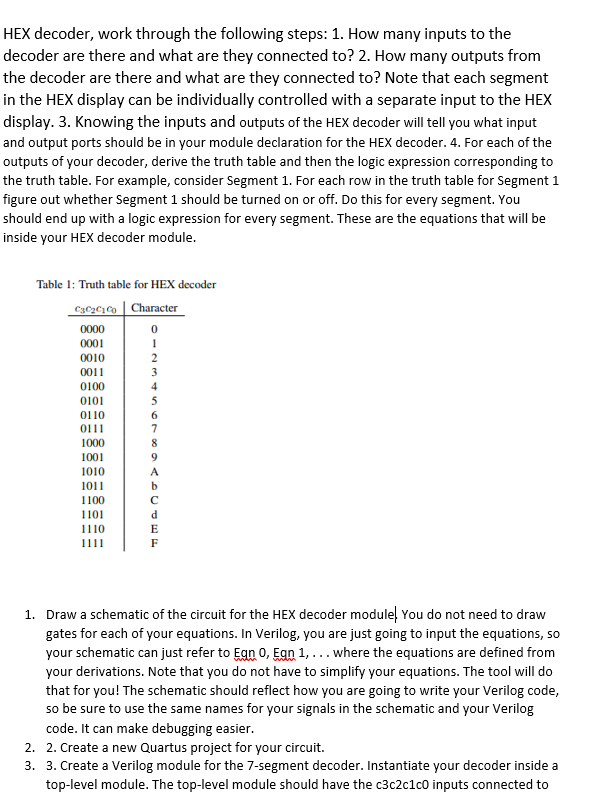
Part 1: Write three separate Verilog modules for the following three 7400-series chips: . 74LS04/05 (six inverters) 74LS08/09 (four 2-input AND gates) 74LS32 (four 2-input OR gates) As a hint, here is an example module declaration for the 74LS04/05: module v7404 (input pin1 pin3, pin5, pin9, pin11, pin13, output pin2, pin4, pin6, pin8, pin10, pin12); After writing and simulating the three 7400-series modules, write another Verilog module that implements a 2-to-1 multiplexer using the three 7400-series modules. You will need one instance of each of your three 7400-series modules. The reason is that the logic function for the 2-to-1 multiplexer is: m = s,x + sy, which requires NOT, AND, and OR. Note that although the 2 to-1 multiplexer will not use all of the internal gates of each 7400- series module, the 7400- series modules should be complete and contain all of the functionality of the original corresponding 7400-series chip. Using "named-port" instantiation will allow you to ignore the unused gates in the 7400-series chips in your top-level design of the 2-to-1 multiplexer 1. Draw a schematic showing how you will connect the three 7400-series modules to build the 2-to-1 multiplexer. Your schematic should have a top-level module that represents the 2-to-1 multiplexer and inside the top-level module you should instantiate each of the 7400-series modules. Give names to all the wires that you need to make the connections and give names to all the instances of the 7400-series modules. Label the used pin names on each module 2. After drawing your schematic, write the Verilog code that corresponds to your schematic. Your Verilog code should use the same names for the wires and instances shown in the schematic. In total, you should have four Verilog modules. 2. 3. 3. Create a new Quartus project for your circuit 4. Simulate the 7400-series modules and the top-level module with ModelSim for different input values. Do enough simulations to convince yourself that the circuit is working Part 2: You are to design a HEX decoder for the 7-segment HEX display (text Section 2.8.3) as shown in Figure 2. In general, a decoder is a circuit that takes an input pattern and converts (decodes) it into a different pattern. A HEX decoder determines how to drive a HEX display according to the value at the input of the decoder as shown in Table 1. You should create a module for the HEX decoder so that you can instantiate it each time you need to drive a HEX display, i.e., instantiate one HEX decoder for every HEX display you are using. You will also use the HEX decoder in future labs because we always want to display output number. To figure out the circuit for the Part 1: Write three separate Verilog modules for the following three 7400-series chips: . 74LS04/05 (six inverters) 74LS08/09 (four 2-input AND gates) 74LS32 (four 2-input OR gates) As a hint, here is an example module declaration for the 74LS04/05: module v7404 (input pin1 pin3, pin5, pin9, pin11, pin13, output pin2, pin4, pin6, pin8, pin10, pin12); After writing and simulating the three 7400-series modules, write another Verilog module that implements a 2-to-1 multiplexer using the three 7400-series modules. You will need one instance of each of your three 7400-series modules. The reason is that the logic function for the 2-to-1 multiplexer is: m = s,x + sy, which requires NOT, AND, and OR. Note that although the 2 to-1 multiplexer will not use all of the internal gates of each 7400- series module, the 7400- series modules should be complete and contain all of the functionality of the original corresponding 7400-series chip. Using "named-port" instantiation will allow you to ignore the unused gates in the 7400-series chips in your top-level design of the 2-to-1 multiplexer 1. Draw a schematic showing how you will connect the three 7400-series modules to build the 2-to-1 multiplexer. Your schematic should have a top-level module that represents the 2-to-1 multiplexer and inside the top-level module you should instantiate each of the 7400-series modules. Give names to all the wires that you need to make the connections and give names to all the instances of the 7400-series modules. Label the used pin names on each module 2. After drawing your schematic, write the Verilog code that corresponds to your schematic. Your Verilog code should use the same names for the wires and instances shown in the schematic. In total, you should have four Verilog modules. 2. 3. 3. Create a new Quartus project for your circuit 4. Simulate the 7400-series modules and the top-level module with ModelSim for different input values. Do enough simulations to convince yourself that the circuit is working Part 2: You are to design a HEX decoder for the 7-segment HEX display (text Section 2.8.3) as shown in Figure 2. In general, a decoder is a circuit that takes an input pattern and converts (decodes) it into a different pattern. A HEX decoder determines how to drive a HEX display according to the value at the input of the decoder as shown in Table 1. You should create a module for the HEX decoder so that you can instantiate it each time you need to drive a HEX display, i.e., instantiate one HEX decoder for every HEX display you are using. You will also use the HEX decoder in future labs because we always want to display output number. To figure out the circuit for the
Step by Step Solution
There are 3 Steps involved in it

Get step-by-step solutions from verified subject matter experts