Please show all work legibly and thanks so much for the explanation! Will rate when I get to it! : )
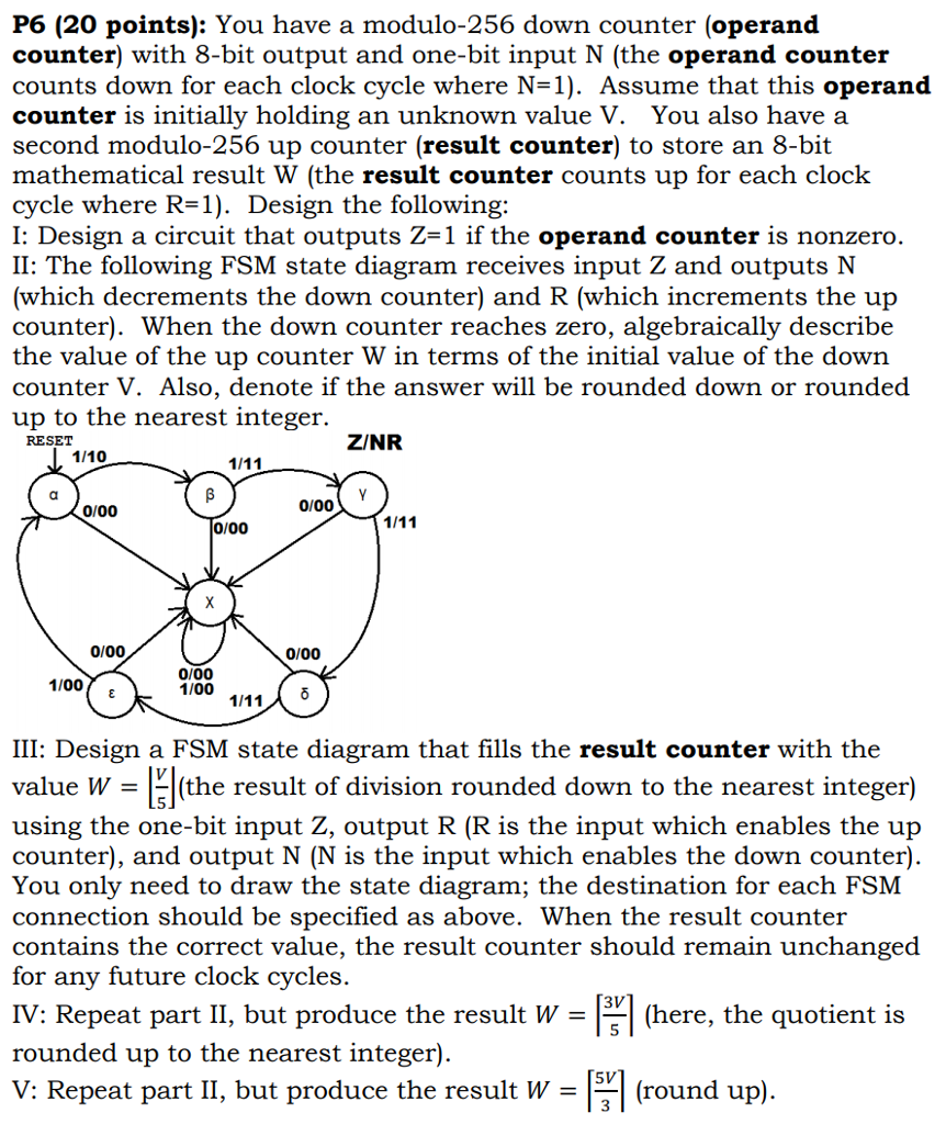
P6 (20 points): You have a modulo-256 down counter (operand counter) with 8-bit output and one-bit input N (the operand counter counts down for each clock cycle where N-1). Assume that this operand counter is initially holding an unknown value V. You also have a second modulo-256 up counter (result counter) to store an 8-bit mathematical result W (the result counter counts up for each clock cycle where R-1). Design the following: I: Design a circuit that outputs Z-1 if the operand counter is nonzero. II: The following FSM state diagram receives input Z and outputs N (which decrements the down counter) and R (which increments the up counter). When the down counter reaches zero, algebraically describe the value of the up counter W in terms of the initial value of the down counter V. Also, denote if the answer will be rounded down or rounded up to the nearest integer RESET ZINR 1/10 0/00 0/00 0/00 0/00 0/00 1100 11 100 ( III: Design a FSM state diagram that fills the result counter with the value W = (the result of division rounded down to the nearest integer) using the one-bit input Z. output R (R is the input which enables the up counter), and output N (N is the input which enables the down counter) You only need to draw the state diagram; the destination for each FSM connection should be specified as above. When the result counter contains the correct value, the result counter should remain unchanged for any future clock cycles. 5 3V IV: Repeat part II, but produce the result W rounded up to the nearest integer). V: Repeat part II, but produce the result W-(round up (here, the quotient is 5V P6 (20 points): You have a modulo-256 down counter (operand counter) with 8-bit output and one-bit input N (the operand counter counts down for each clock cycle where N-1). Assume that this operand counter is initially holding an unknown value V. You also have a second modulo-256 up counter (result counter) to store an 8-bit mathematical result W (the result counter counts up for each clock cycle where R-1). Design the following: I: Design a circuit that outputs Z-1 if the operand counter is nonzero. II: The following FSM state diagram receives input Z and outputs N (which decrements the down counter) and R (which increments the up counter). When the down counter reaches zero, algebraically describe the value of the up counter W in terms of the initial value of the down counter V. Also, denote if the answer will be rounded down or rounded up to the nearest integer RESET ZINR 1/10 0/00 0/00 0/00 0/00 0/00 1100 11 100 ( III: Design a FSM state diagram that fills the result counter with the value W = (the result of division rounded down to the nearest integer) using the one-bit input Z. output R (R is the input which enables the up counter), and output N (N is the input which enables the down counter) You only need to draw the state diagram; the destination for each FSM connection should be specified as above. When the result counter contains the correct value, the result counter should remain unchanged for any future clock cycles. 5 3V IV: Repeat part II, but produce the result W rounded up to the nearest integer). V: Repeat part II, but produce the result W-(round up (here, the quotient is 5V