Answered step by step
Verified Expert Solution
Question
1 Approved Answer
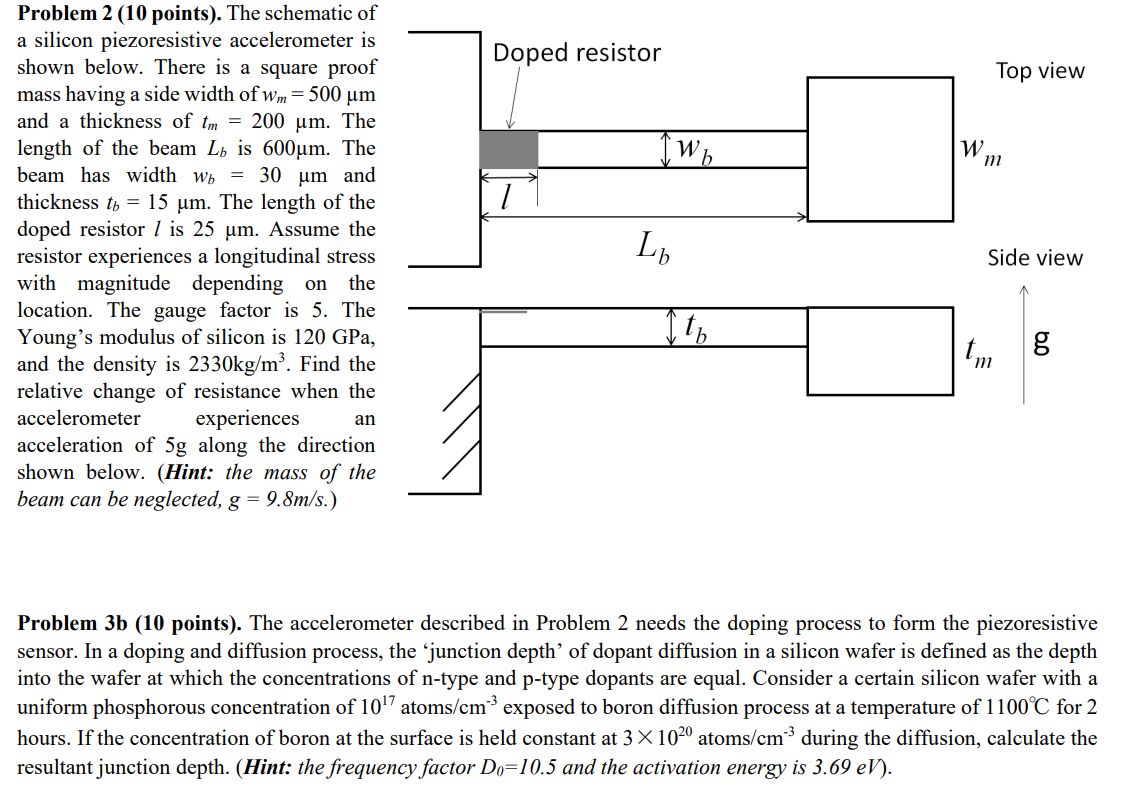
Problem 2 (10 points). The schematic of a silicon piezoresistive accelerometer is shown below. There is a square proof mass having a side width

Problem 2 (10 points). The schematic of a silicon piezoresistive accelerometer is shown below. There is a square proof mass having a side width of wm = 500 m and a thickness of tm = 200 m. The length of the beam L is 600m. The beam has width w = 30 m and thickness t = 15 m. The length of the doped resistor is 25 m. Assume the resistor experiences a longitudinal stress with magnitude depending on the location. The gauge factor is 5. The Young's modulus of silicon is 120 GPa, and the density is 2330kg/m. Find the relative change of resistance when the accelerometer experiences acceleration of 5g along the direction shown below. (Hint: the mass of the beam can be neglected, g = 9.8m/s.) an Doped resistor Lb Wh W m Top view Side view It b tm g 60 Problem 3b (10 points). The accelerometer described in Problem 2 needs the doping process to form the piezoresistive sensor. In a doping and diffusion process, the 'junction depth' of dopant diffusion in a silicon wafer is defined as the depth into the wafer at which the concentrations of n-type and p-type dopants are equal. Consider a certain silicon wafer with a uniform phosphorous concentration of 107 atoms/cm exposed to boron diffusion process at a temperature of 1100C for 2 hours. If the concentration of boron at the surface is held constant at 31020 atoms/cm during the diffusion, calculate the resultant junction depth. (Hint: the frequency factor Do=10.5 and the activation energy is 3.69 eV).
Step by Step Solution
There are 3 Steps involved in it
Step: 1

Get Instant Access to Expert-Tailored Solutions
See step-by-step solutions with expert insights and AI powered tools for academic success
Step: 2

Step: 3

Ace Your Homework with AI
Get the answers you need in no time with our AI-driven, step-by-step assistance
Get Started


