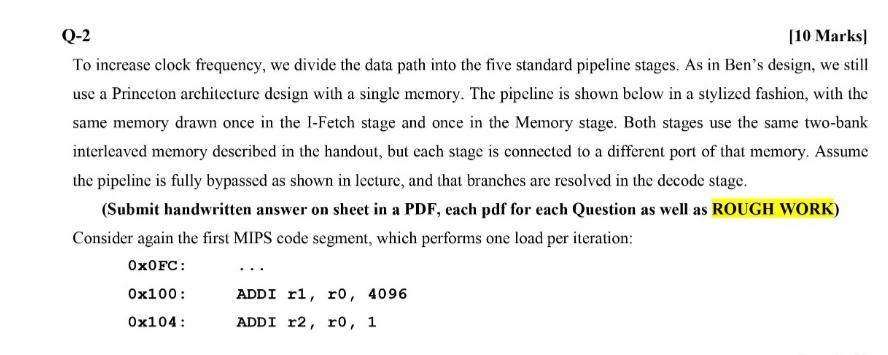
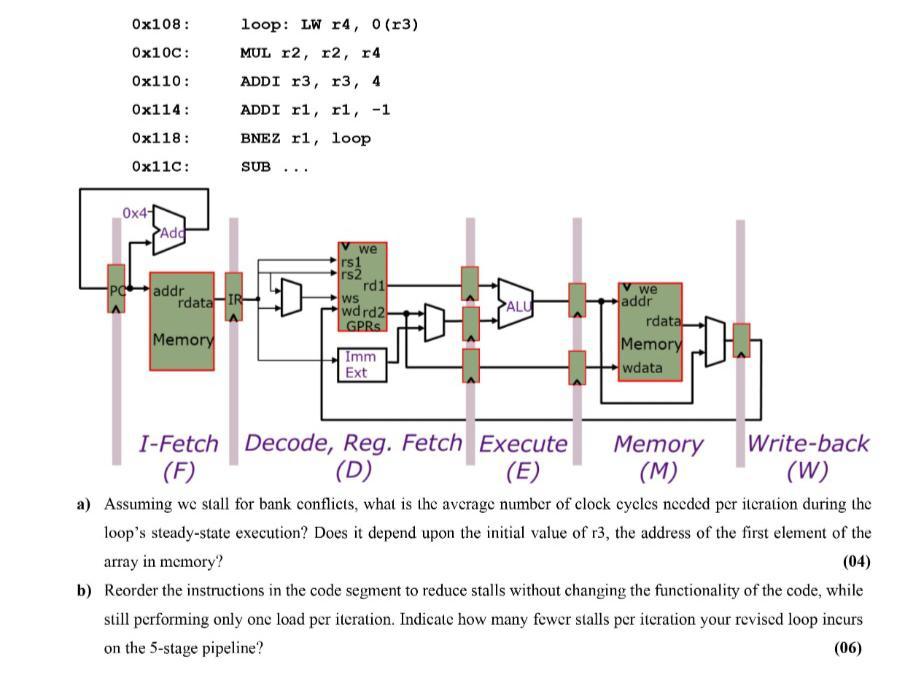
Q-2 [10 Marks) To increase clock frequency, we divide the data path into the five standard pipeline stages. As in Ben's design, we still use a Princeton architecture design with a single memory. The pipeline is shown below in a stylized fashion, with the same memory drawn once in the l-Fetch stage and once in the Memory stage. Both stages use the same two-bank interleaved memory described in the handout, but each stage is connected to a different port of that memory. Assume the pipeline is fully bypassed as shown in lecture, and that branches are resolved in the decode stage. (Submit handwritten answer on sheet in a PDF, each pdf for each Question as well as ROUGH WORK) Consider again the first MIPS code segment, which performs one load per iteration: Ox0FC: 0x100: ADDI ri, ro, 4096 Ox104: ADDI r2, ro, 1 Ox108 : Ox10C: 0x110: Ox114: loop: LW r4, 0(r3) MUL r2, r2, r4 ADDI r3, r3 4 ADDI ri, r1, -1 BNEZ ri, loop Ox118: Ox11c: SUB ... 0x47 >Add -PC addr we rs 1 rs2 rd 1 WS wdrd2 GPRS we rdata IR ALU Memory addr rdata Memory wdata Imm Ext 1-Fetch Decode, Reg. Fetch Execute Memory Write-back (F) (D) (E) (M) (W) a) Assuming wc stall for bank conflicts, what is the average number of clock cycles needed per iteration during the loop's steady-state execution? Does it depend upon the initial value of r3, the address of the first element of the array in memory? (04) b) Reorder the instructions in the code segment to reduce stalls without changing the functionality of the code, while still performing only onc load per iteration. Indicate how many fewer stalls per iteration your revised loop incurs on the 5-stage pipeline? (06) Q-2 [10 Marks) To increase clock frequency, we divide the data path into the five standard pipeline stages. As in Ben's design, we still use a Princeton architecture design with a single memory. The pipeline is shown below in a stylized fashion, with the same memory drawn once in the l-Fetch stage and once in the Memory stage. Both stages use the same two-bank interleaved memory described in the handout, but each stage is connected to a different port of that memory. Assume the pipeline is fully bypassed as shown in lecture, and that branches are resolved in the decode stage. (Submit handwritten answer on sheet in a PDF, each pdf for each Question as well as ROUGH WORK) Consider again the first MIPS code segment, which performs one load per iteration: Ox0FC: 0x100: ADDI ri, ro, 4096 Ox104: ADDI r2, ro, 1 Ox108 : Ox10C: 0x110: Ox114: loop: LW r4, 0(r3) MUL r2, r2, r4 ADDI r3, r3 4 ADDI ri, r1, -1 BNEZ ri, loop Ox118: Ox11c: SUB ... 0x47 >Add -PC addr we rs 1 rs2 rd 1 WS wdrd2 GPRS we rdata IR ALU Memory addr rdata Memory wdata Imm Ext 1-Fetch Decode, Reg. Fetch Execute Memory Write-back (F) (D) (E) (M) (W) a) Assuming wc stall for bank conflicts, what is the average number of clock cycles needed per iteration during the loop's steady-state execution? Does it depend upon the initial value of r3, the address of the first element of the array in memory? (04) b) Reorder the instructions in the code segment to reduce stalls without changing the functionality of the code, while still performing only onc load per iteration. Indicate how many fewer stalls per iteration your revised loop incurs on the 5-stage pipeline? (06)