

Question: QUESTION 1 a . Design implementation in the FPGA design flow for digital systems is a process by which the circuit descriped at generic logic
QUESTION
a Design implementation in the FPGA design flow for digital systems is a process by which the circuit descriped at generic logic gates level is turned into a configuration logic blocs or logic elements that define the FPGA devices in use Xilinx Altera, At this step, a static timing pts analysis is perfomed and a timing simulation can be done using the generated back annotation file. What is the purpose of such file?
b In designing digital circuits what is the difference between abstraction levels and domain of
abstraction
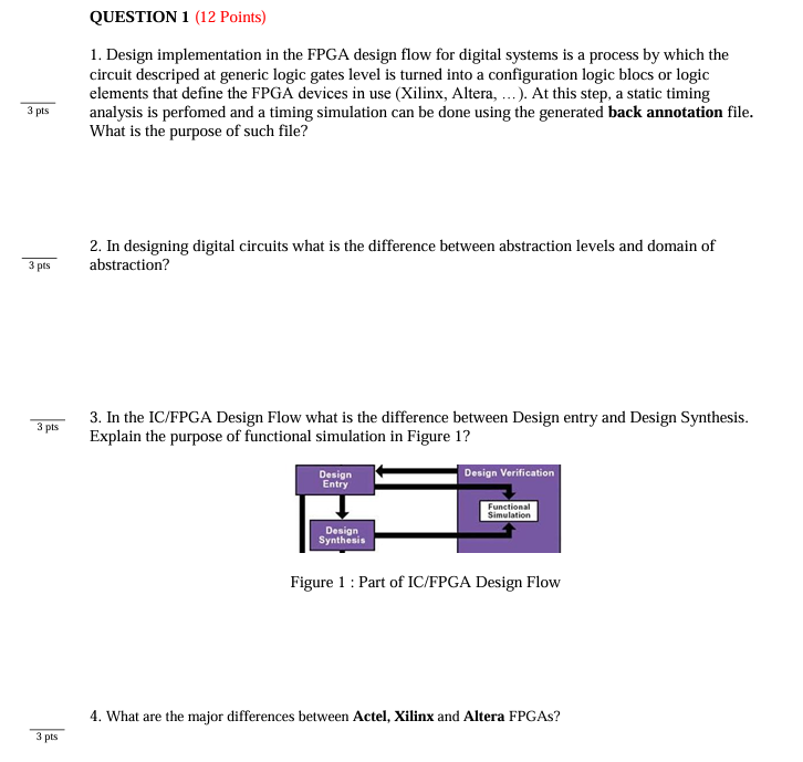
c In the ICFPGA Design Flow what is the difference between Design entry and Design Synthesis. Explain the purpose of functional simulation in Figure
Figure : Part of ICFPGA Design Flow
d What are the major differences between Actel, Xilinx and Altera FPGAs?
Step by Step Solution
There are 3 Steps involved in it
1 Expert Approved Answer
Step: 1 Unlock

Question Has Been Solved by an Expert!
Get step-by-step solutions from verified subject matter experts
Step: 2 Unlock
Step: 3 Unlock