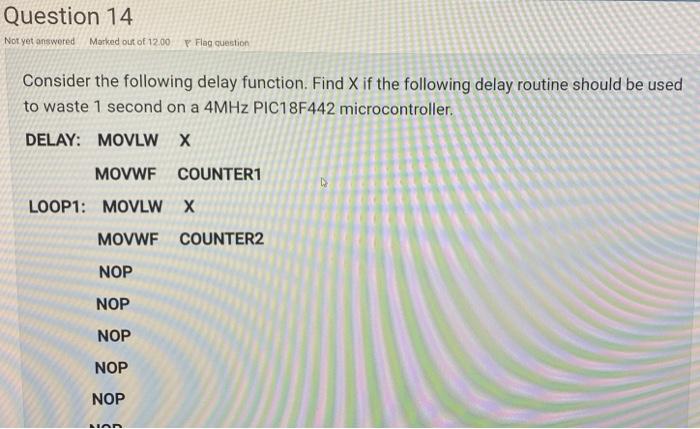
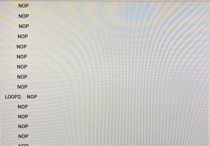
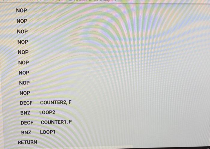
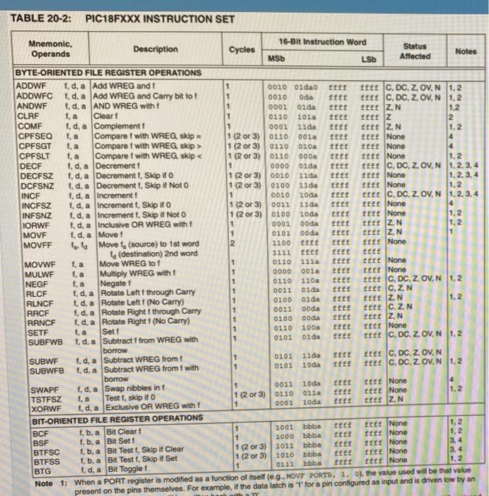
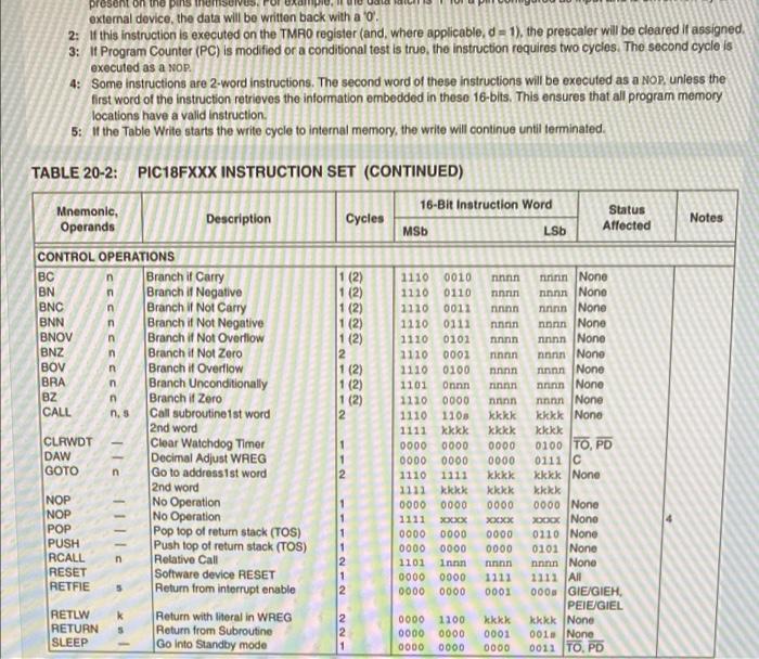
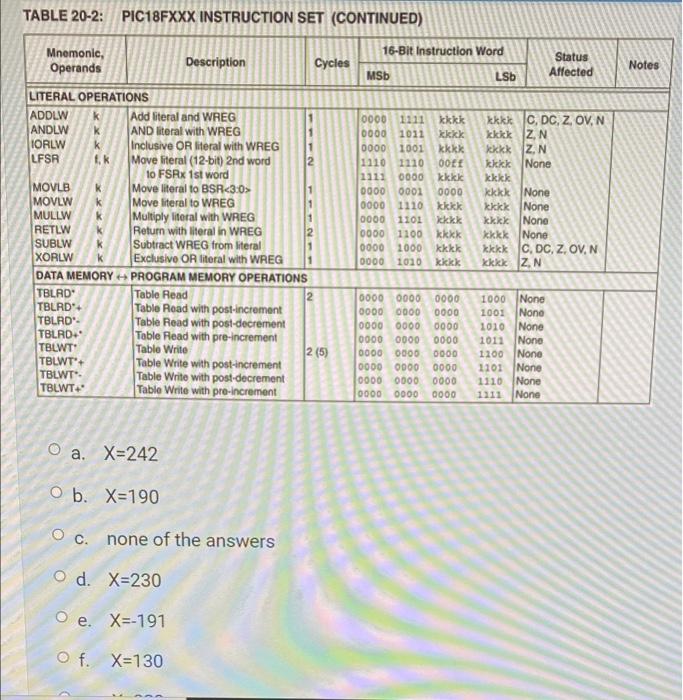
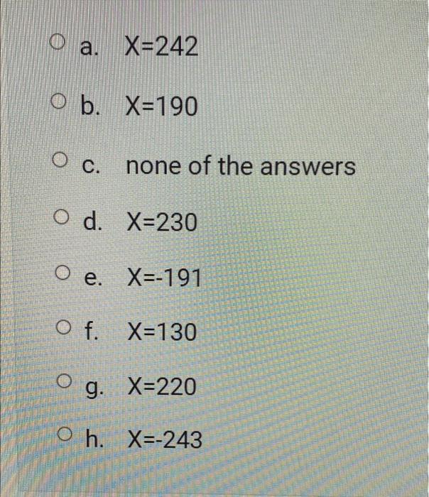
Question 14 Not yet answered Marked out of 12.00 F Flag question Consider the following delay function. Find X if the following delay routine should be used to waste 1 second on a 4MHz PIC18F442 microcontroller. DELAY: MOVLW X MOVWF COUNTER1 LOOP1: MOVLW X MOVWF COUNTER2 NOP NOP NOP NOP NOP SIAN NOP NOP NOP NOP NOP NOP NOP NOP NOP LOOP2: NOP NOP NOP NOP NOP Man NOP NOP NOP NOP NOP NOP NOP NOP NOP DECF COUNTER2, F BNZ LOOP2 DECF COUNTER1, F BNZ LOOP1 RETURN TABLE 20-2: PIC18FXXX INSTRUCTION SET MSD NON 1.2 Mnemonic, 16-Bit Instruction Word Description Operands Cycles Status Notes LSD Affected BYTE-ORIENTED FILE REGISTER OPERATIONS ADDWF 1, d, a Add WREG and 1 0010 Oldao EEEE ADDWFC EEEE C, DC, Z, OV, N 1,2 1. d, a Add WREG and Carry bit to 0010 Oda EEEE IEEE C, DC, Z, OV, N 1,2 ANDWF 1.d, a AND WREG with 1 0001 01da FEE CLRF EEEE ZN 1.2 f.a Clear 0110 101a EEEE EEEE Z 2 COMF I, d, a Complement 1 0001 11 da IEEE EEE ZN 1.2 CPFSEQ f.a Compare f with WREG skip 1 (2 or 3) 0110 vola EEEE FEEE None 4 CPFSGT 1, a Compare f with WREG Skip > 1 (2 or 3) 0120 010 IEEE EEEE None 4 CPFSLT 1, a Compare with WREG skip 1 (2 or 3) 0110 000 EEEE Et None DECF 1,2 1.d, a Decrement 1 0000 01 da EEEE EEEE C, DC, Z. OVN 1.2.3.4 DECFSZ 1.d, a Decrement 1, Skip to 1 (2 or 3)0010 11 da EEEE IEEE None 1.2.3.4 DCFSNZ 1.d, a Decrement 1, Skip it Not O 1 (2 or 3) 0100 11 da EEEE IEEE None 1.2 INCF f.d, a Increment 1 0010 10da TELE EEEE C, DC, Z. OV, N 1,2,3,4 INCFSZ 1. d, a increment 1, Skip ifo 1 (2 or 3) 0011 12 da IEEE IEEE None 4 INFSNZ 1. d. a Increment 1, Skip it Not O 1 (2 or 3) 0100 10da Eitt FECE None 1.2 IORWF 1. d, a Inclusive OR WREG with 1 0001 ooda EEEE IEEE ZN MOVE f. d, a Move 1 1 0102 ooda EEEE IEEE IZN MOVFF Isla Move t, (source) to 1st word 2 1100 EEEE IEEE EECE None 1s (destination) 2nd word 1111 EEEE EEEE FEE MOVWF f, a Move WREG to f 0110 111a fert fEEt None MULWF f, a Multiply WREG with 0000 001a CE None NEGF f.a Negatet 0110 1100 EEEE EEE C, DC, Z, OV, N 1.2 RLCF 1.d, a Rotate Left through Carry 0012 olda EECE Ett C,ZN RLNCF 1. d, a Rotate Leftf (No Carry) 0100 olda CERE EEEE ZN 1.2 RRCF t.d, a Rotate Right f through Carry 0011 ooda IEEE PECE CZN RRNCF f.d, a Rotate Right 1 (No Carry) 0100 Ooda EEEE IEEE ZN SETF 1, a Sett 0110 100 EEEE ECE None SUBFWB 1. d, a Subtract f from WREG with 0101 01da EEEE Et C, DC, Z OVN 1.2 borrow SUBWF 1. d, a Subtract WREG from 0101 11 da tett C, DC. Z. OVN SUBWFB 0101 10da LEEE 1.d, a Subtract WREG from with fett C. DC, Z. OVN 1.2 borrow 1 SWAPF 4 0011 10da IEEE None EEEE f, d, a Swap nibbles inf 011a EEEE TSTFSZ 1 (2 or 3) 0110 f.a Test , skip if o IEEE None 1 10da 0001 PECE XORWF IEEE ZN 1, d. a Exclusive OR WREG with BIT-ORIENTED FILE REGISTER OPERATIONS EEEE 1 1,2 1001 bbba EEEF None BCF f. b, a Bit Clear 1 bbba IEEE None 1000 1,2 BSF 1. b, a Bit Set 1 2011 bbba 1 (2 or 3) EEEE 3.4 FECE None BTFSC 1. b, a Bit Testt, Skip it Clear 1010 bbba FEE 1 (2 or 3) 3.4 FEEL None BTFSS f, b, a Bit Test 1, Skip it Set 0111 1 bbba 1.2 ferr None BTG 1.d, a Bit Toggle Note 1: When a PORT register is modified as a function of itself (e.g.MOVF PORTS. 1.0), the value used will be that value present on the pins themselves. For example, if the data latch is '1' for a pin configured as input and is driven low by an 1.2 HU present on the pins external device, the data will be written back with a '0. 2: If this instruction is executed on the TMRO register (and, where applicable, d = 1), the prescaler will be cleared if assigned 3: It Program Counter (PC) is modified or a conditional test is true, the instruction requires two cycles. The second cycle is executed as a NOP. 4: Some instructions are 2-word instructions. The second word of these instructions will be executed as a NOP, unless the first word of the instruction retrieves the information embedded in these 16-bits. This ensures that all program memory locations have a valid instruction 5: If the Table Write starts the write cycle to internal memory, the write will continue until terminated. Notes 11 (2) 1 (2) n TABLE 20-2: PIC18FXXX INSTRUCTION SET (CONTINUED) Mnemonie, 16-Bit Instruction Word Status Description Cycles Operands MSb LSD Affected CONTROL OPERATIONS BC n Branch it Carry 11 (2) 1110 0010 nnnn nurinn None BN n Branch it Negative 1110 0110 nnnn nnnn None BNC n Branch if Not Carry 1 (2) 1110 0012 nnnn nnnn None BNN n Branch if Not Negative 1110 0111 nnnn nnnn None BNOV n Branch if Not Overflow 1 (2) 1110 0102 nnnn nnnn None BNZ in Branch if Not Zero 12 2110 0001 nnnn nnnn None BOV Branch it Overflow 1 (2) 1110 0100 nnnn inn None BRA n Branch Unconditionally 1 (2) 1101 Onnn nnnn nnnn None BZ Branch if Zoro 1 (2) 1110 0000 nnnn nnnn None CALL Call subroutine 1st word 2 1110 1108 kkkk kkkk None 2nd word 1111 kkkk kkkk kkkk CLRWDT Clear Watchdog Timer 1 0000 0000 0000 0100 TO, PD DAW Decimal Adjust WREG 0000 0000 0000 0111 C GOTO Go to address ist word 2 1110 1111 kkkk kkkk None 2nd word 1112 kkkk kkkk kkkk NOP No Operation 0000 0000 0000 0000 None NOP No Operation 1111 00XX XXXX DOGC None POP Pop top of return stack (TOS) 0000 0000 0000 0110 None PUSH Push top of return stack (TOS) 0000 0000 0000 0101 None RCALL Relative Call 1101 Innn nnnn nnnn None RESET Software device RESET 0000 0000 1111 1111 All RETFIE Return from interrupt enable 0000 0000 0001 000 GIE/GIEH PEIE/GIEL RETLW K Return with literal in WREG 2 0000 1100 kkkk kkkk None RETURN Return from Subroutine 0000 0000 0001 001. None SLEEP Go into Standby mode 0000 0000 0000 0011 TO.PD ns cells llis NN- TABLE 20-2: PIC18FXXX INSTRUCTION SET (CONTINUED) Notes Mnemonic, 16-Bit Instruction Word Status Operands Description Cycles Affected MSb LSD LITERAL OPERATIONS ADDLW k Add literal and WREG 0000 1111 kkkk kkkk C, DC, Z, OV, N ANDLW AND literal with WREG 0000 1011 kkkk kkkk ZN IORLW k Inclusive OR literal with WREG 0000 1001 kkkk kkkk ZN LFSR EK Move literal (12-bit) 2nd word 2 1110 1110 00Ft kkkk None 10 FSRX 1st word 1111 0000 kkkk kkkk MOVLB K Move literal to BSR 0000 0001 0000 kkkk None MOVLW k Move literal to WREG 0000 1110 kkkk kkkk None MULLW k Multiply literal with WREG 0000 1101 kkkk kkkk None RETLW K Return with literal in WREG 0000 1100 kkkk kkkk None SUBLW K Subtract WREG from literal 0000 1000 kkkk kkkk C, DC, Z. OV, N XORLW Exclusive OR literal with WREG 1 0000 1010 kkkk kkkk ZN DATA MEMORY - PROGRAM MEMORY OPERATIONS TBLRD Table Read 2 00000000 0000 1000 None TBLRD+ Table Read with post-increment 0000 0000 0000 1001 Nono TBLRD' Table Read with post-docrement 0000 0000 0000 1010 None TBLRD. Table Read with pre-increment 0000 0000 0000 1011 None TBLWT Table Write 2 (5) 0000 0000 0000 1200 None TBLWT- Table Write with post-increment 00000000 0000 1101 None TBLWT Table Write with post-docrement 0000 0000 0000 1110 None TBLWT Table Write with pre-increment 0000 0000 0000 1111 None O a. X=242 O b. X=190 C. none of the answers O d. X=230 O e. X=-191 O f. X=130 O a. X=242 o b. X=190 O c. none of the answers O d. X=230 O e. X=-191 O f. X=130 O g. X=220 Oh. X=-243 Question 14 Not yet answered Marked out of 12.00 F Flag question Consider the following delay function. Find X if the following delay routine should be used to waste 1 second on a 4MHz PIC18F442 microcontroller. DELAY: MOVLW X MOVWF COUNTER1 LOOP1: MOVLW X MOVWF COUNTER2 NOP NOP NOP NOP NOP SIAN NOP NOP NOP NOP NOP NOP NOP NOP NOP LOOP2: NOP NOP NOP NOP NOP Man NOP NOP NOP NOP NOP NOP NOP NOP NOP DECF COUNTER2, F BNZ LOOP2 DECF COUNTER1, F BNZ LOOP1 RETURN TABLE 20-2: PIC18FXXX INSTRUCTION SET MSD NON 1.2 Mnemonic, 16-Bit Instruction Word Description Operands Cycles Status Notes LSD Affected BYTE-ORIENTED FILE REGISTER OPERATIONS ADDWF 1, d, a Add WREG and 1 0010 Oldao EEEE ADDWFC EEEE C, DC, Z, OV, N 1,2 1. d, a Add WREG and Carry bit to 0010 Oda EEEE IEEE C, DC, Z, OV, N 1,2 ANDWF 1.d, a AND WREG with 1 0001 01da FEE CLRF EEEE ZN 1.2 f.a Clear 0110 101a EEEE EEEE Z 2 COMF I, d, a Complement 1 0001 11 da IEEE EEE ZN 1.2 CPFSEQ f.a Compare f with WREG skip 1 (2 or 3) 0110 vola EEEE FEEE None 4 CPFSGT 1, a Compare f with WREG Skip > 1 (2 or 3) 0120 010 IEEE EEEE None 4 CPFSLT 1, a Compare with WREG skip 1 (2 or 3) 0110 000 EEEE Et None DECF 1,2 1.d, a Decrement 1 0000 01 da EEEE EEEE C, DC, Z. OVN 1.2.3.4 DECFSZ 1.d, a Decrement 1, Skip to 1 (2 or 3)0010 11 da EEEE IEEE None 1.2.3.4 DCFSNZ 1.d, a Decrement 1, Skip it Not O 1 (2 or 3) 0100 11 da EEEE IEEE None 1.2 INCF f.d, a Increment 1 0010 10da TELE EEEE C, DC, Z. OV, N 1,2,3,4 INCFSZ 1. d, a increment 1, Skip ifo 1 (2 or 3) 0011 12 da IEEE IEEE None 4 INFSNZ 1. d. a Increment 1, Skip it Not O 1 (2 or 3) 0100 10da Eitt FECE None 1.2 IORWF 1. d, a Inclusive OR WREG with 1 0001 ooda EEEE IEEE ZN MOVE f. d, a Move 1 1 0102 ooda EEEE IEEE IZN MOVFF Isla Move t, (source) to 1st word 2 1100 EEEE IEEE EECE None 1s (destination) 2nd word 1111 EEEE EEEE FEE MOVWF f, a Move WREG to f 0110 111a fert fEEt None MULWF f, a Multiply WREG with 0000 001a CE None NEGF f.a Negatet 0110 1100 EEEE EEE C, DC, Z, OV, N 1.2 RLCF 1.d, a Rotate Left through Carry 0012 olda EECE Ett C,ZN RLNCF 1. d, a Rotate Leftf (No Carry) 0100 olda CERE EEEE ZN 1.2 RRCF t.d, a Rotate Right f through Carry 0011 ooda IEEE PECE CZN RRNCF f.d, a Rotate Right 1 (No Carry) 0100 Ooda EEEE IEEE ZN SETF 1, a Sett 0110 100 EEEE ECE None SUBFWB 1. d, a Subtract f from WREG with 0101 01da EEEE Et C, DC, Z OVN 1.2 borrow SUBWF 1. d, a Subtract WREG from 0101 11 da tett C, DC. Z. OVN SUBWFB 0101 10da LEEE 1.d, a Subtract WREG from with fett C. DC, Z. OVN 1.2 borrow 1 SWAPF 4 0011 10da IEEE None EEEE f, d, a Swap nibbles inf 011a EEEE TSTFSZ 1 (2 or 3) 0110 f.a Test , skip if o IEEE None 1 10da 0001 PECE XORWF IEEE ZN 1, d. a Exclusive OR WREG with BIT-ORIENTED FILE REGISTER OPERATIONS EEEE 1 1,2 1001 bbba EEEF None BCF f. b, a Bit Clear 1 bbba IEEE None 1000 1,2 BSF 1. b, a Bit Set 1 2011 bbba 1 (2 or 3) EEEE 3.4 FECE None BTFSC 1. b, a Bit Testt, Skip it Clear 1010 bbba FEE 1 (2 or 3) 3.4 FEEL None BTFSS f, b, a Bit Test 1, Skip it Set 0111 1 bbba 1.2 ferr None BTG 1.d, a Bit Toggle Note 1: When a PORT register is modified as a function of itself (e.g.MOVF PORTS. 1.0), the value used will be that value present on the pins themselves. For example, if the data latch is '1' for a pin configured as input and is driven low by an 1.2 HU present on the pins external device, the data will be written back with a '0. 2: If this instruction is executed on the TMRO register (and, where applicable, d = 1), the prescaler will be cleared if assigned 3: It Program Counter (PC) is modified or a conditional test is true, the instruction requires two cycles. The second cycle is executed as a NOP. 4: Some instructions are 2-word instructions. The second word of these instructions will be executed as a NOP, unless the first word of the instruction retrieves the information embedded in these 16-bits. This ensures that all program memory locations have a valid instruction 5: If the Table Write starts the write cycle to internal memory, the write will continue until terminated. Notes 11 (2) 1 (2) n TABLE 20-2: PIC18FXXX INSTRUCTION SET (CONTINUED) Mnemonie, 16-Bit Instruction Word Status Description Cycles Operands MSb LSD Affected CONTROL OPERATIONS BC n Branch it Carry 11 (2) 1110 0010 nnnn nurinn None BN n Branch it Negative 1110 0110 nnnn nnnn None BNC n Branch if Not Carry 1 (2) 1110 0012 nnnn nnnn None BNN n Branch if Not Negative 1110 0111 nnnn nnnn None BNOV n Branch if Not Overflow 1 (2) 1110 0102 nnnn nnnn None BNZ in Branch if Not Zero 12 2110 0001 nnnn nnnn None BOV Branch it Overflow 1 (2) 1110 0100 nnnn inn None BRA n Branch Unconditionally 1 (2) 1101 Onnn nnnn nnnn None BZ Branch if Zoro 1 (2) 1110 0000 nnnn nnnn None CALL Call subroutine 1st word 2 1110 1108 kkkk kkkk None 2nd word 1111 kkkk kkkk kkkk CLRWDT Clear Watchdog Timer 1 0000 0000 0000 0100 TO, PD DAW Decimal Adjust WREG 0000 0000 0000 0111 C GOTO Go to address ist word 2 1110 1111 kkkk kkkk None 2nd word 1112 kkkk kkkk kkkk NOP No Operation 0000 0000 0000 0000 None NOP No Operation 1111 00XX XXXX DOGC None POP Pop top of return stack (TOS) 0000 0000 0000 0110 None PUSH Push top of return stack (TOS) 0000 0000 0000 0101 None RCALL Relative Call 1101 Innn nnnn nnnn None RESET Software device RESET 0000 0000 1111 1111 All RETFIE Return from interrupt enable 0000 0000 0001 000 GIE/GIEH PEIE/GIEL RETLW K Return with literal in WREG 2 0000 1100 kkkk kkkk None RETURN Return from Subroutine 0000 0000 0001 001. None SLEEP Go into Standby mode 0000 0000 0000 0011 TO.PD ns cells llis NN- TABLE 20-2: PIC18FXXX INSTRUCTION SET (CONTINUED) Notes Mnemonic, 16-Bit Instruction Word Status Operands Description Cycles Affected MSb LSD LITERAL OPERATIONS ADDLW k Add literal and WREG 0000 1111 kkkk kkkk C, DC, Z, OV, N ANDLW AND literal with WREG 0000 1011 kkkk kkkk ZN IORLW k Inclusive OR literal with WREG 0000 1001 kkkk kkkk ZN LFSR EK Move literal (12-bit) 2nd word 2 1110 1110 00Ft kkkk None 10 FSRX 1st word 1111 0000 kkkk kkkk MOVLB K Move literal to BSR 0000 0001 0000 kkkk None MOVLW k Move literal to WREG 0000 1110 kkkk kkkk None MULLW k Multiply literal with WREG 0000 1101 kkkk kkkk None RETLW K Return with literal in WREG 0000 1100 kkkk kkkk None SUBLW K Subtract WREG from literal 0000 1000 kkkk kkkk C, DC, Z. OV, N XORLW Exclusive OR literal with WREG 1 0000 1010 kkkk kkkk ZN DATA MEMORY - PROGRAM MEMORY OPERATIONS TBLRD Table Read 2 00000000 0000 1000 None TBLRD+ Table Read with post-increment 0000 0000 0000 1001 Nono TBLRD' Table Read with post-docrement 0000 0000 0000 1010 None TBLRD. Table Read with pre-increment 0000 0000 0000 1011 None TBLWT Table Write 2 (5) 0000 0000 0000 1200 None TBLWT- Table Write with post-increment 00000000 0000 1101 None TBLWT Table Write with post-docrement 0000 0000 0000 1110 None TBLWT Table Write with pre-increment 0000 0000 0000 1111 None O a. X=242 O b. X=190 C. none of the answers O d. X=230 O e. X=-191 O f. X=130 O a. X=242 o b. X=190 O c. none of the answers O d. X=230 O e. X=-191 O f. X=130 O g. X=220 Oh. X=-243
