

Answered step by step
Verified Expert Solution
Question
1 Approved Answer
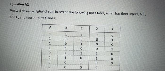
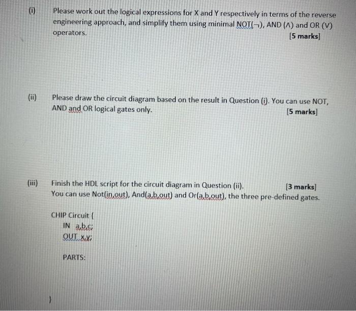
Question A2 We will design a digital circuit, based on the following truth table, which has three inputs, A, B, and C, and two outputs
Step by Step Solution
There are 3 Steps involved in it
Step: 1

Get Instant Access to Expert-Tailored Solutions
See step-by-step solutions with expert insights and AI powered tools for academic success
Step: 2

Step: 3
Ace Your Homework with AI
Get the answers you need in no time with our AI-driven, step-by-step assistance
Get Started
Database Design Application And Administration
Authors: Michael Mannino, Michael V. Mannino
2nd Edition
0072880678, 9780072880670