

Question
Question Absorption and emission of light in crystalline materials. Semiconductor crystals (pure silicon or germanium) are commonly used to detect IR, visible, UV and X-ray
Question
Absorption and emission of light in crystalline materials. Semiconductor crystals (pure silicon or germanium) are commonly used to detect IR, visible, UV and X-ray light. The energy gap between the valence and conduction bands in silicon crystal is 1.14 eV and in germanium crystal 0.67 eV. In the photoeffect in the valence band, the photoelectron is ejected into the conduction band. When a voltage is connected to the crystal, the electric field drives an electric current of electrons along the conduction band, and an electric current of positively charged gaps flows through the valence band. In this way, we can detect that light has been absorbed in the crystal and measure the incident flux of light.
a) What is the longest (limit) wavelength of light that can still be absorbed in these two crystals? b) What should be the energy gap in the crystal for the detector to detect only UV light and not visible and IR?
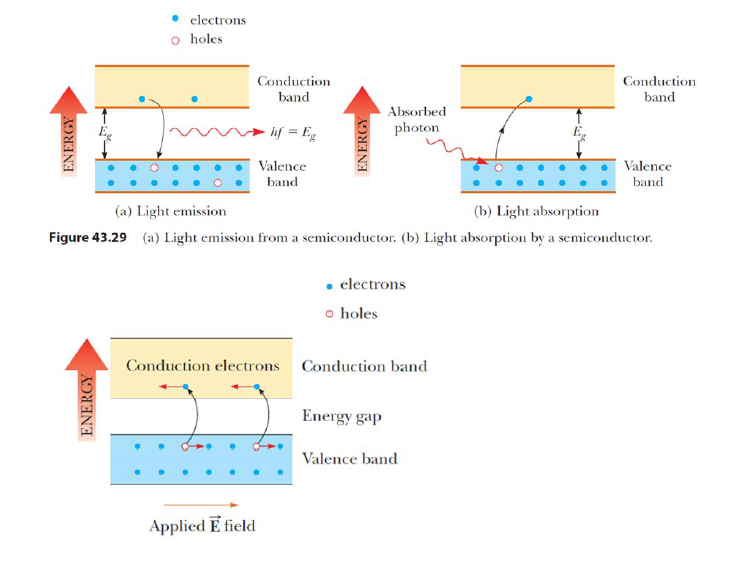 - electrons holes (a) Light emission (b) Light absorption Figure 43.29 (a) Light emission from a semiconductor. (b) Light absorption by a semiconductor: - electrons holes Conduction band Energy gap Valence band Applied E field
 Step by Step Solution
There are 3 Steps involved in it
Step: 1

Get Instant Access to Expert-Tailored Solutions
See step-by-step solutions with expert insights and AI powered tools for academic success
Step: 2

Step: 3
Ace Your Homework with AI
Get the answers you need in no time with our AI-driven, step-by-step assistance
Get Started
Water Quality Engineering Physical Chemical Treatment Processes
Authors: Mark M. Benjamin, Desmond F. Lawler
1st Edition
1118169654, 9781118169650