

Question: For the following common-emitter amplifier: R R ww www Vcc= 10 V Rc 10 km2 Q2N2222 RE 1.0 1.1 1.2 1.8 1.3 (a) Use
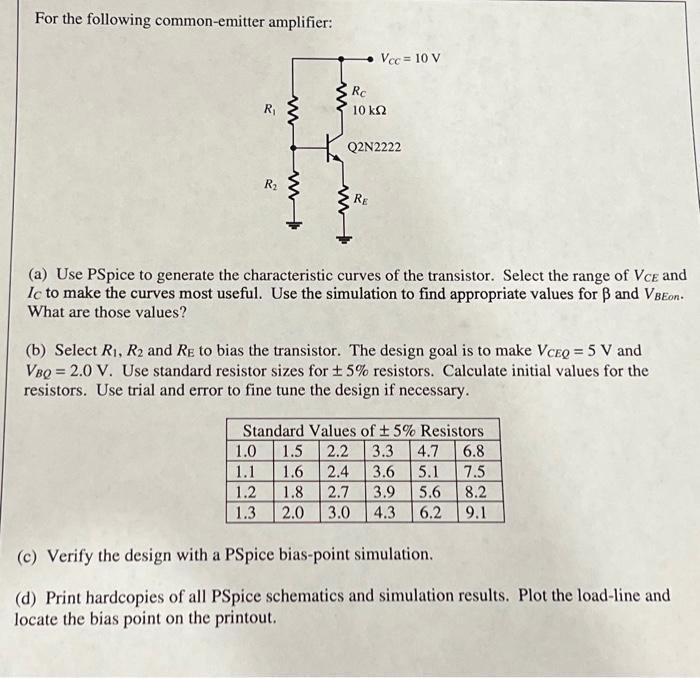
For the following common-emitter amplifier: R R ww www Vcc= 10 V Rc 10 km2 Q2N2222 RE 1.0 1.1 1.2 1.8 1.3 (a) Use PSpice to generate the characteristic curves of the transistor. Select the range of VCE and Ic to make the curves most useful. Use the simulation to find appropriate values for B and VBEon- What are those values? (b) Select R, R2 and RE to bias the transistor. The design goal is to make VCEQ = 5 V and VBQ = 2.0 V. Use standard resistor sizes for 5% resistors. Calculate initial values for the resistors. Use trial and error to fine tune the design if necessary. Standard Values of 5% Resistors 1.5 2.2 3.3 4.7 6.8 1.6 2.4 3.6 5.1 7.5 2.7 3.9 5.6 8.2 2.0 3.0 4.3 6.2 9.1 (c) Verify the design with a PSpice bias-point simulation. (d) Print hardcopies of all PSpice schematics and simulation results. Plot the load-line and locate the bias point on the printout.
Step by Step Solution
3.47 Rating (147 Votes )
There are 3 Steps involved in it
a Generating the characteristic curves of the transistor To generate the characteristic curves of the transistor we can use a simple PSpice schematic ... View full answer

Get step-by-step solutions from verified subject matter experts