

Testbench module you need to use for testing:
module adcinterface_tb();
parameter N = 12; // Number of ADC bits (LTC2308 is a 12-bit ADC)
logic clk, reset_n; // clock and reset logic [2:0] chan; // channel to be sampled logic [N-1:0] result; // result read by adc interface module logic [N-1:0] adcoutput = 0; // randomly generated ADC output logic [N-1:0] configword = 0; // capture configuration word from adcinterface // ltc2308 signals logic ADC_CONVST, ADC_SCK, ADC_SDI; logic ADC_SDO = 0;
adcinterface dut_0 (.*); // device under test
initial begin clk = 0; reset_n = 0; chan = 0; // hold in reset for two clock cycles repeat(2) @(posedge clk); reset_n = 1; // loop for each possible channel do begin
// wait for conversion start signal @(posedge ADC_CONVST); // generate a random n-bit ADC output adcoutput = $urandom_range('hfff, 0);
for (int i = N-1; i>=0; i--) begin // place each data bit on SDO and wait for negative edge of serial clock to change output ADC_SDO = adcoutput[i]; @(posedge ADC_SCK); // capture config word on positive edge configword[i] = ADC_SDI; @(negedge ADC_SCK); end repeat(2) @(posedge clk); // check that results matches the serial data transmitted by ADC module $display ("%s: expected ADC ouput %3h, received %3h", adcoutput == result ? "PASS" : "FAIL", adcoutput, result); // verify that correct configuration word is sent for the selected channel $display ("%s: channel %1d, expected config word %2h, received %2h", configword[N-1:6] == {1'b1, chan[0], chan[2:1], 1'b1, 1'b0} ? "PASS" : "FAIL", chan, {1'b1, chan[0], chan[2:1], 1'b1, 1'b0}, configword[N-1:6]);
chan++; end while (chan != 0); $stop;
end
// generate clock always #1ms clk = ~clk;
endmodule
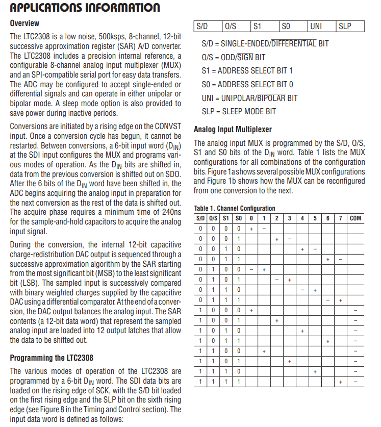
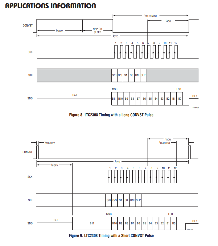
page 10 and page 17 for 2308fb datasheet:


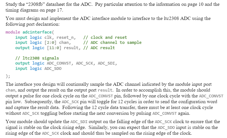
VerilogQuestion Verilog Question Verilog Question Verilog Question Verilog Question Verilog Question Verilog Question Verilog Question Verilog Question Verilog Question Verilog Question Verilog Question Verilog Question Verilog Question VerilogQuestion VerilogQuestion Verilog Question Verilog Question Verilog Question Verilog Question Verilog Question Verilog Question Verilog Question Verilog Question Verilog Question Verilog Question Verilog Question Verilog Question Verilog Question Verilog Question Verilog Question Verilog Question Verilog Question Verilog Question Verilog Question Verilog Qustion Study the 2308fb datasheet for the ADC. Pay particular attention to the information on page 10 and the timing diagrams on page 17. You must design and implement the ADC interface module to interface to the Itc2308 ADC using the following port declaration: module adcinterface input logic clk, reset_n, // clock and reset input logic (2:0] chan, // ADC channel to sample output logic (11:0] result, // ADC result // ltc2308 signals output logic ADC_CONVST, ADC_SCK, ADC_SDI, input logic ADC_SDO ); The interface you design will continually sample the ADC channel indicated by the module input port chan, and output the result on the output port result. In order to accomplish this, the module should output a pulse for one clock cycle on the ADC_CONVST pin, followed by one clock cycle with the ADC_CONVST pin low. Subsequently, the ADC_SCK pin will toggle for 12 cycles in order to send the configuration word and capture the result data. Following the 12 cycle data transfer, there must be at least one clock cycle without ADC_SCK toggling before starting the next conversion by pulsing ADC_CONVST again. Your module should update the ADC_SDI output on the falling edge of the ADC_SCK clock to ensure that the signal is stable on the clock rising edge. Similarly, you can expect that the ADC_SDo input is stable on the rising edge of the ADC_SCK clock and should thus be sampled on the rising edge of the clock. In order to "gate the clock output to the ADC_SCK signal, you may want to use a statement similar to: assign ADC_SCK = (state == ????) ? clk : 1'be; Simulate your ADC interface design using the testbench provided. Below is a sample waveform showing what your output might look like. 2.000 Icon u0101112 1000L01L00... Madonace_thick 10 aconterface_b/resu 1 /ascinerace_th/chan 0.10 fodlone lucr_lb/resul 110000100110 anteracc_th/edcoutput 100101100110 food for th/chard 11001000000 /adamterface_tbADC_CONVST 0 adainterface th/ADC SOX D fasonierface_b/ADC_509 V Vladicinterface th/ADC 5DO 0 0.000000 DODANDA 180111011COD 100000000000 70001000000 10009102112 11100.00 . LIZZLE Z7LAnnnnnnnn Once all tests pass, save a copy of the simulation results portion of the Transcript window and take a snapshot of your waveform to submit with the lab. APPLICATIONS INFORMATION Overview S/D O/S S1 SO UNI SLP The LTC2308 is a low noise, 500ksps, 8-channel, 12-bit successive approximation register (SAR) A/D converter. S/D = SINGLE-ENDED/DIFFERENTIAL BIT The LTC2308 includes a precision internal reference, a 0/S = ODD/SIGN BIT configurable 8-channel analog input multiplexer (MUX) S1 = ADDRESS SELECT BIT 1 and an SPl-compatible serial port for easy data transfers. The ADC may be configured to accept single-ended or SO = ADDRESS SELECT BITO differential signals and can operate in either unipolar or UNI = UNIPOLAR/BIPOLAR BIT bipolar mode. A sleep mode option is also provided to save power during inactive periods. SLP = SLEEP MODE BIT Conversions are initiated by a rising edge on the CONVST Analog Input Multiplexer input. Once a conversion cycle has begun, it cannot be restarted. Between conversions, a 6-bit input word (DIN) The analog input MUX is programmed by the S/D, O/S, at the SDI input configures the MUX and programs vari- S1 and So bits of the Din word. Table 1 lists the MUX ous modes of operation. As the Din bits are shifted in, configurations for all combinations of the configuration data from the previous conversion is shifted out on SDO bits. Figure 1a shows several possible MUX configurations After the 6 bits of the Din word have been shifted in, the and Figure 1b shows how the MUX can be reconfigured ADC begins acquiring the analog input in preparation for from one conversion to the next. the next conversion as the rest of the data is shifted out. The acquire phase requires a minimum time of 240ns Table 1. Channel Configuration for the sample-and-hold capacitors to acquire the analog SD 0/8 S1 SO 0 1 2 3 4 5 6 input signal. 0 0 0 During the conversion, the internal 12-bit capacitive 00 charge-redistribution DAC output is sequenced through a successive approximation algorithm by the SAR starting from the most significant bit (MSB) to the least significant bit (LSB). The sampled input is successively compared with binary weighted charges supplied by the capacitive DAC using a differential comparator. At the end of a conver- sion, the DAC output balances the analog input. The SAR 0 contents (a 12-bit data word) that represent the sampled analog input are loaded into 12 output latches that allow the data to be shifted out. 011 00 Programming the LTC2308 101 The various modes of operation of the LTC2308 are programmed by a 6-bit Din word. The SDI data bits are loaded on the rising edge of SCK, with the S/D bit loaded on the first rising edge and the SLP bit on the sixth rising edge (see Figure 8 in the Timing and Control section). The input data word is defined as follows: 7 COM 0 + 0 0 0 1 1 0 0 1 1 + 0 1 0 0 + 0 1 0 1 0 1 1 0 0 1 1 1 0 0 + PIPI 0 0 1 1 0 1 0 + 1 + 1 1 + 1 1 1 1 0 APPLICATIONS INFORMATION LWLCONVST taco CONVST ICON NAP OR SLEEP 1 2 3 4 5 6 7 8 9 10 11 12 SCK FULLLLLLLL SDI S/DO/SS1 SOUNI SLP MSB LSB Hi-Z Hi-Z SDO B9B8B7B6 B5 B4 B3 B2 B1 BO 20 FOR Figure 8. LTC2308 Timing with a Long CONVST Pulse taca THCONVST -WHCONV CONVST tcc CONV 2 3 4 5 6 7 8 9 10 11 12 ATLLALLAHU ANHA SCK SDI SD OS S1 SOUNI SLP MSB LSB Hi-Z Hi-Z SDO B11 B10 B9B8B7B6 85 84 83 B2 B1 BO 230 POS Figure 9. LTC2308 Timing with a Short CONVST Pulse VerilogQuestion Verilog Question Verilog Question Verilog Question Verilog Question Verilog Question Verilog Question Verilog Question Verilog Question Verilog Question Verilog Question Verilog Question Verilog Question Verilog Question VerilogQuestion VerilogQuestion Verilog Question Verilog Question Verilog Question Verilog Question Verilog Question Verilog Question Verilog Question Verilog Question Verilog Question Verilog Question Verilog Question Verilog Question Verilog Question Verilog Question Verilog Question Verilog Question Verilog Question Verilog Question Verilog Question Verilog Qustion Study the 2308fb datasheet for the ADC. Pay particular attention to the information on page 10 and the timing diagrams on page 17. You must design and implement the ADC interface module to interface to the Itc2308 ADC using the following port declaration: module adcinterface input logic clk, reset_n, // clock and reset input logic (2:0] chan, // ADC channel to sample output logic (11:0] result, // ADC result // ltc2308 signals output logic ADC_CONVST, ADC_SCK, ADC_SDI, input logic ADC_SDO ); The interface you design will continually sample the ADC channel indicated by the module input port chan, and output the result on the output port result. In order to accomplish this, the module should output a pulse for one clock cycle on the ADC_CONVST pin, followed by one clock cycle with the ADC_CONVST pin low. Subsequently, the ADC_SCK pin will toggle for 12 cycles in order to send the configuration word and capture the result data. Following the 12 cycle data transfer, there must be at least one clock cycle without ADC_SCK toggling before starting the next conversion by pulsing ADC_CONVST again. Your module should update the ADC_SDI output on the falling edge of the ADC_SCK clock to ensure that the signal is stable on the clock rising edge. Similarly, you can expect that the ADC_SDo input is stable on the rising edge of the ADC_SCK clock and should thus be sampled on the rising edge of the clock. In order to "gate the clock output to the ADC_SCK signal, you may want to use a statement similar to: assign ADC_SCK = (state == ????) ? clk : 1'be; Simulate your ADC interface design using the testbench provided. Below is a sample waveform showing what your output might look like. 2.000 Icon u0101112 1000L01L00... Madonace_thick 10 aconterface_b/resu 1 /ascinerace_th/chan 0.10 fodlone lucr_lb/resul 110000100110 anteracc_th/edcoutput 100101100110 food for th/chard 11001000000 /adamterface_tbADC_CONVST 0 adainterface th/ADC SOX D fasonierface_b/ADC_509 V Vladicinterface th/ADC 5DO 0 0.000000 DODANDA 180111011COD 100000000000 70001000000 10009102112 11100.00 . LIZZLE Z7LAnnnnnnnn Once all tests pass, save a copy of the simulation results portion of the Transcript window and take a snapshot of your waveform to submit with the lab. APPLICATIONS INFORMATION Overview S/D O/S S1 SO UNI SLP The LTC2308 is a low noise, 500ksps, 8-channel, 12-bit successive approximation register (SAR) A/D converter. S/D = SINGLE-ENDED/DIFFERENTIAL BIT The LTC2308 includes a precision internal reference, a 0/S = ODD/SIGN BIT configurable 8-channel analog input multiplexer (MUX) S1 = ADDRESS SELECT BIT 1 and an SPl-compatible serial port for easy data transfers. The ADC may be configured to accept single-ended or SO = ADDRESS SELECT BITO differential signals and can operate in either unipolar or UNI = UNIPOLAR/BIPOLAR BIT bipolar mode. A sleep mode option is also provided to save power during inactive periods. SLP = SLEEP MODE BIT Conversions are initiated by a rising edge on the CONVST Analog Input Multiplexer input. Once a conversion cycle has begun, it cannot be restarted. Between conversions, a 6-bit input word (DIN) The analog input MUX is programmed by the S/D, O/S, at the SDI input configures the MUX and programs vari- S1 and So bits of the Din word. Table 1 lists the MUX ous modes of operation. As the Din bits are shifted in, configurations for all combinations of the configuration data from the previous conversion is shifted out on SDO bits. Figure 1a shows several possible MUX configurations After the 6 bits of the Din word have been shifted in, the and Figure 1b shows how the MUX can be reconfigured ADC begins acquiring the analog input in preparation for from one conversion to the next. the next conversion as the rest of the data is shifted out. The acquire phase requires a minimum time of 240ns Table 1. Channel Configuration for the sample-and-hold capacitors to acquire the analog SD 0/8 S1 SO 0 1 2 3 4 5 6 input signal. 0 0 0 During the conversion, the internal 12-bit capacitive 00 charge-redistribution DAC output is sequenced through a successive approximation algorithm by the SAR starting from the most significant bit (MSB) to the least significant bit (LSB). The sampled input is successively compared with binary weighted charges supplied by the capacitive DAC using a differential comparator. At the end of a conver- sion, the DAC output balances the analog input. The SAR 0 contents (a 12-bit data word) that represent the sampled analog input are loaded into 12 output latches that allow the data to be shifted out. 011 00 Programming the LTC2308 101 The various modes of operation of the LTC2308 are programmed by a 6-bit Din word. The SDI data bits are loaded on the rising edge of SCK, with the S/D bit loaded on the first rising edge and the SLP bit on the sixth rising edge (see Figure 8 in the Timing and Control section). The input data word is defined as follows: 7 COM 0 + 0 0 0 1 1 0 0 1 1 + 0 1 0 0 + 0 1 0 1 0 1 1 0 0 1 1 1 0 0 + PIPI 0 0 1 1 0 1 0 + 1 + 1 1 + 1 1 1 1 0 APPLICATIONS INFORMATION LWLCONVST taco CONVST ICON NAP OR SLEEP 1 2 3 4 5 6 7 8 9 10 11 12 SCK FULLLLLLLL SDI S/DO/SS1 SOUNI SLP MSB LSB Hi-Z Hi-Z SDO B9B8B7B6 B5 B4 B3 B2 B1 BO 20 FOR Figure 8. LTC2308 Timing with a Long CONVST Pulse taca THCONVST -WHCONV CONVST tcc CONV 2 3 4 5 6 7 8 9 10 11 12 ATLLALLAHU ANHA SCK SDI SD OS S1 SOUNI SLP MSB LSB Hi-Z Hi-Z SDO B11 B10 B9B8B7B6 85 84 83 B2 B1 BO 230 POS Figure 9. LTC2308 Timing with a Short CONVST Pulse

